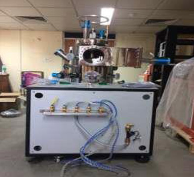
The Inter-University Accelerator Centre in houses the “Pelletron Accelerator” along with the low energy ion beam facility (LEIBF) and negative implanter facility, provides a unique opportunity for researchers to study the field of Ion Induced Materials Engineering and Characterization. There are two dedicated beamlines in the respective beamhalls (BH-I and Beam Hall-II) for irradiation studies with accelarated ions from Pelletron and Linac. The beamline in Pelletron beamhall (BH-I) includes two irradiation chambers with on-line ERDA, on-line RGA and ionoluminiscence facilities. Low flux irradiation facility for materials science is also available in another beamline (GPSC). The beamline in Linac beamhall (BH-II) has two irradiation chambers with on-line ERDA and in-situ XRD facility. In-situ Raman facility is also integrated.
Insitu/online facilities
- Elastic Recoil Detection Analysis setups
- Ionoluminescence Setup
- Micro-Raman Setup
- Residual Gas Analysis Setup
- X-ray diffractometer
Offline facilities
- Electrical Transport/Noise measurements setup
- FTIR
- Micro-Raman Setup
- Photoluminescence Setup
- Scanning Electron Microscopy
- Scanning Probe Microscopy
- Transmission Electron Microscopy
- UV-Vis absorption spectrophotometer
- X-ray diffractometer
- Contact Angle Set-up
Synthesis facilities
- Atom beam sputtering
- Ball-milling
- Box Furnace
- D. C. Sputter deposition
- Thermal evaporation: Setup1 Setup2
- Thermal evaporation for electrical contact
- ECR plasma based deposition
- RF Sputtering
- Tube Furnace
Facilities Under Material Science
The materials science beamlines support research programmes of a large number of users from different universities and institutions. Though the swift heavy ion (SHI) irradiation and related experiments mostly utilize irradiation chamber in the materials science beamlines in beamhall-I using Pelletron accelerator, experiments utilizing in-situ XRD and in-situ Raman facility and those using beams from LINAC are performed in the materials science beamline in beamhall-II. Besides this studies requiring low fluence irradiation for fluencesas low as 103ions/cm2to 107ions/cm2are performed in GPSC beamline.
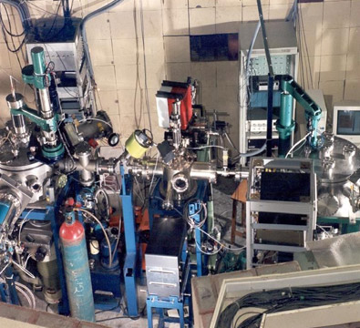
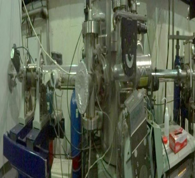
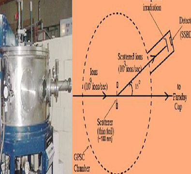
Low flux ion irradiations are perfomed in General Purpose ScatteringChamber(GPSC) beamline Low energy ion irradiations experimentsare performed in Low Energy Ion Beam Facility (LEIBF) and Negative Ion Implanter Facility.
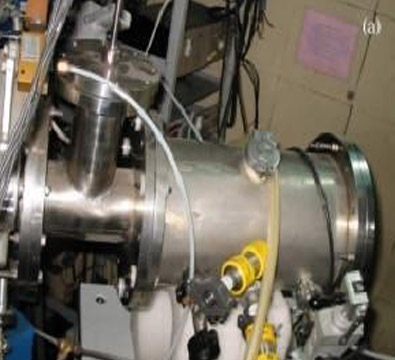
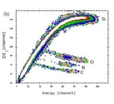
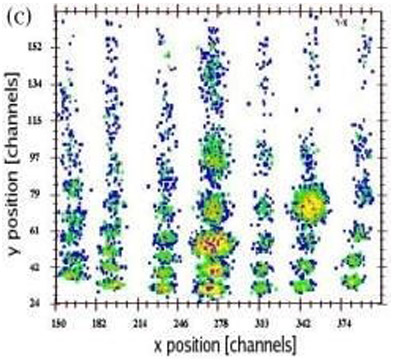
Large area position sensitive gaseous detector telescopes, developed and were installed in both the beam halls at IUAC, are used in on-line measurement of SHI induced compositional changes. The detector shown in Fig. (a) is fixed to a 45° port of the high vacuum chamber of materials science beam line in Beam Hall I. The detector offers good Z resolution as shown in Fig. (b) which shows a bi-dimensional ΔE-E recoil spectrum recorded for a silicon oxy-nitride sample. The ΔE1 signal discriminates very well between the recoils of adjacent masses like C, N, O as in this example. The two-dimensional position spectra recorded during facility test using 120 MeV Ag ions is shown in Fig. (c). The position sensitivity in scattering plane is around 0.1° which is good enough for correcting the kinematic broadening of the detector (~17% in the present ERD geometry due to the large acceptance of the detector). ERDA setup in beam hall II has been dismantled.
Some publications:
- On Development
- S. A. Khan, Manvendra Kumar, D.K. Avasthi, Development of a position sensitive detector telescope for ERDA based on-line monitoring of swift heavy ions induced modifications, Nucl. Instr. and Meth. B. 266 (2008) 1912
- S. V. S. Nageswara Rao, A. Kothari, G. B. V. S. Lakshmi, S. A. Khan, Ambuj Tripathi, Azher M. Siddiqui, Anand P. Pathak, and D. K. Avasthi, Development of a large area two dimensional position sensitive ΔE-E detector telescope for material analysis, Nucl. Instr. and Meth. B 212 (2003) 545
- Studies utilizing ERDA setups at IUAC
- R.K. Bommali, S. Ghosh, S.A. Khan, P. Srivastava, Hydrogen loss and its improved retention in hydrogen plasma treated a-SiNx:H films: ERDA study with 100 MeV Ag7+ ions, Nucl. Instrum. Methods Phys. Res., Sect. B, 423 (2018) 16-21.
- V.S. Vendamani, S.A. Khan, M. Dhanunjaya, A.P. Pathak, S.V.S.N. Rao, Energetic ion induced desorption of hydrogen from porous silicon studied by on-line elastic recoil detection analysis, Microporous Mesoporous Mater., 246 (2017) 81-88.
- D. Sarker, S. Ghosh, P. Srivastava, Spectral weight shift in the valence band density of states and concurrent increase in field emission by hydrogenation of FeCo–SiO2 nanocomposites, RSC Advances, 5 (2015) 63377-63381.
- V. Singh, B.R. Mehta, S.K. Sengar, P.K. Kulriya, S.A. Khan, S.M. Shivaprasad, Enhanced Hydrogenation Properties of Size Selected Pd–C Core–Shell Nanoparticles; Effect of Carbon Shell Thickness, The Journal of Physical Chemistry C, 119 (2015) 14455-14460.
- R.K. Bommali, S. Ghosh, G. Vijaya Prakash, K. Gao, S. Zhou, S.A. Khan, P. Srivastava, Hydrogen plasma induced modification of photoluminescence from a-SiNx:H thin films, J. Appl. Phys., 115 (2014) 053525.
- S.K. Sengar, B.R. Mehta, P.K. Kulriya, S.A. Khan, Enhanced hydrogenation and reduced lattice distortion in size selected Pd-Ag and Pd-Cu alloy nanoparticles, Appl. Phys. Lett., 103 (2013) 173107.
- D. Gupta, R. Chauhan, S. Kumar, P. Diwan, S. Khan, A. Tripathi, S. Ghosh, V. Mittal, Nanoscale Track Diameter and Hydrogen Yield: Dependence upon Charge State of Incident Ion on Polystyrene, World Journal of Condensed Matter Physics, 3 (2013) 95-101.
- Pragya Jain, Ankur Jain, Devendra Vyas, D. Kabiraj, S. A. Khan, and I. P. Jain, Comparative study on hydrogenation properties of Pd capped Mg and Mg/Al films, Int. J. Hydrogen Energy 37 (4) (2012) 37793785
- Yogendra K. Gautam, Amit K. Chawla, Saif A. Khan, R. D. Agrawal, and Ramesh Chandra, Hydrogen absorption and optical properties of Pd/Mg thin films prepared by DC magnetron sputtering, Int. J. Hydrogen Energy 37 (4) (2012) 3772-3778
- Fouran Singh, R. G. Singh, Vinod Kumar, S. A. Khan, and J. C. Pivin, Softening of phonons by lattice defects and structural strain in heavy ion irradiated nanocrystalline zinc oxide films, J. Appl. Phys. 110 (8) (2011) 083520
- P. Jain, A. Jain, D. Vyas, R. Verma, S.A. Khan, I.P. Jain, The effects of Ni and Mg2Ni interlayer on hydrogenation properties of Pd sandwiched Mg films, J. Alloys Compd., 509 (2011) 2105-2110.
- S. P. Patel, S. A. Khan, A. K. Chawla, R. Chandra, J. C. Pivin, D. Kanjilal, and L. Kumar, Structural phase diagram for ZnS nanocrystalline thin films under swift heavy ion irradiation, Physica B-Condensed Matter 406 (21) (2011) 4150-4154
- M. Kumar, P. Rajput, S. A. Khan, D. K. Avasthi, A. C. Pandey, Substrate effect on electronic sputtering yield in polycrystalline fluoride (LiF, CaF2 and BaF2 ) thin films, Applied Surface Science 256 (2010) 2199
- Rucha H. Polji, A. D. Yadav, S. K. Dubey, Saif A. Khan, D. K. Avasthi and T. K. Gundu Rao, HI-ERDA, Micro-Raman and HRXRD studies of buried silicon oxynitride layers synthesized by dual ion implantation, Vacuum 83 (2009) 1164
- U. S. Joshi, S. J. Trivedi, K. H. Bhavsar, U. N. Trivedi, S. A. Khan, and D. K. Avasthi, Resistance switching properties of planner Ag/Li:NiO/Ag structures induced by swift heavy ion irradiation, J. of Appl. Phys. 105 (2009) 073704
- Anjali, S. Ghosh, S. A. Khan, P. Srivastava, R. Pal, A. P. Pathak, Study of H loss from hydrogenated Hg1-xCd xTe under high electronic excitation by elastic recoil detection analysis (ERDA), Nucl. Instr. and Meth. B. 267 (2009) 1797
- Sarab Preet Singh, P Srivastava, S Ghosh, Saif A Khan and G Vijaya Prakash, Phase stabilization by rapid thermal annealing in amorphous hydrogenated silicon nitride film, J. Phys.: Condens. Matter 21 (2009) 095010
- D. C. Agarwal, R. S. Chauhan, D. K. Avasthi, S. A. Khan, D. Kabiraj and I. Sulania, Formation of self –affine nanostructures on ZnO surfaces by swift heavy ions, J. Appl. Phys. 104 (2008) 024304
- Y. Batra, S.A. Khan, D. Kabiraj, S. Kumar, D. Kanjilal, Elastic recoil detection (ERD) analysis of GeOx thin films, Nucl. Instr. and Meth. B. 266 (2008) 1697
- Amit Kumar, S. A. Khan, Manvendra Kumar, D. C. Agarwal, Fouran Singh, A. Tripathi, Govind, S. M. Shivaprasad, J. Salomon, L. Pichon, J. C. Pivin and D. K. Avasthi, Oxygen intake in ion irradiated fullerene films, Nucl. Instr. and Meth. B. 266 (2008) 1709.
- A. Tripathi, S.A. Khan, Manvendra Kumar, V. Baranwal, R. Krishna, Sarvesh Kumar, A.C. Pandey, D.K. Avasthi, Angular dependence of electronic sputtering from HOPG, Nucl. Instr. and Meth. B. 266 (2008) 1265
- Shubhra Kala, B. R. Mehta, S. A. Khan, D. K. Avasthi, Nanotracks as transport routes for enhanced and reversible hydrogen diffusion in swift heavy ion irradiated Pd-Pr layers, Appl. Phys. Lett. 90 (2007) 153121
- M. Kumar, S. A. Khan, F. Singh, A Tripathi, D K Avasthi, A C Pandey, Influence of grain size on electronic sputtering of LiF thin films, Nucl. Instr. and Meth. B 256 (2007) 328
- M. Kumar, S. A. Khan, P. Rajput, F. Singh, A. Tripathi, D. K. Avasthi, A. C. Pandey, Size effect on electronic sputtering of LiF thin films, J. Appl. Phys. 102 (2007) 83510
- D. C. Agarwal, R. S. Chauhan, Amit Kumar, D. Kabiraj, F. Singh, S. A. Khan, D. K. Avasthi, J. C. Pivin, M. Kumar, J. Ghatak, and P. V. Satyam, Synthesis and characterization of ZnO thin film grown by electron beam evaporation, J. Appl. Phys. 99 (2006) 123105
- A. Kumar, F. Singh, S. A. Khan, D. C. Agarwal, A. Tripathi, D. K. Avasthi, J. C. Pivin,Precipitation of semiconducting carbon nanoparticles in ion irradiated gels, Nucl. Instr. and Meth. B 244 (2006) 23
- S. Ghosh, V. V. Sivakumar, A. Tripathi, S. Khan, V. Ganesan, A. Gupta, A. Nath, D. K. Avasthi,Formation of nanoscale metallic structures on cupric nitride thin film surface by the impact of 200MeV Au15+ ions, Nucl. Instrum. and Methods in Phys. Res. B 248 (2006) 71
- S. Kumar, R. S. Chauhan, S. A. Khan, W. Bolse, D. K. Avasthi, Swift heavy ion induced mixing in metal/metal system, Nucl. Instr. and Meth. B 244 (2006) 194
- S. Ghosh, D. K. Avasthi, A. Tripathi, D. Kabiraj, P. Sugathan, G. K. Chaudhary, and P. Barua,Heavy ion elastic recoil detection analysis set up for electronic sputtering studies, Rad. Eff. and Defects in Solids 161 (2006) 247
- D. K. Avasthi and W. Assmann, ERDA with swift heavy ions for materials characterization,Current Science 80 (2001) 1532
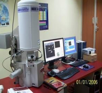
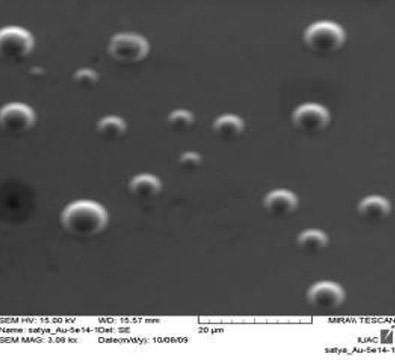
A field emission scanning electron microscope (FE-SEM): MIRA II LMH from TESCAN, with a resolution of 1.5 nm at 30 kV has been installed to boost research activities in nanomaterials, in a project funded under Nano Initiative program of Department of Science and Technology. It has a secondary electron (SE) and a backscattered electron (BSE) detector for imaging. An energy dispersive X ray detector INCA PentaFET3 with 133 eV resolution from OXFORD has also been installed in this system for elemental analysis.
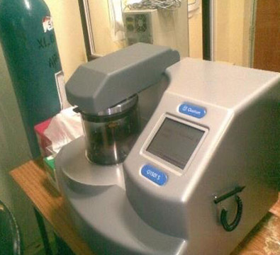
Sputter Coater System for FE-SEM
To improve the performance and applicability to different types of samples, Q150T-S High Vacuum Turbo pumped Sputter Coater system from Quoram Technologies has been installed. The system is regularly being used to coat the samples with gold, carbon and chromium.
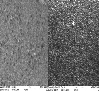
The SEM facility is being heavily utilized for characterization of samples of IUAC users. Some of the publications which benefited from this facility are listed below.
2019
- S.K. Patla, M. Mukhopadhyay, R. Ray, P. Maiti, A.K. Mukhopadhyay, D. Sen, K. Asokan, Non-suitability of high-energy (MeV) irradiation for property enhancement of structurally stable poly (ethylene oxide) polyvinylidene fluoride blend bromide composite electrolyte membrane, Ionics, 25 (2019) 2159-2170.
- A. Chattaraj, S. Khan, L. Walczak, A. Kanjilal, Probing the impact of surface reactivity on charge transport in dimensional phase changed tungsten films, Journal of Materials Science: Materials in Electronics, 30 (2019) 8278-8285.
- K. Asha, A. Banerjee, S. Saxena, S.A. Khan, I. Sulaniya, V.R. Satsangi, R. Shrivastav, R. Kant, S. Dass, Morphological influence of electrode/electrolyte interface towards augmenting the efficiency of photoelectrochemical water splitting – A case study on ZnO, Journal of Power Sources, 432 (2019) 38-47.
2018
- P. Yadav, S. Rattan, A. Tripathi, S. Kumar, Cost effective Fe/NG/PMMA nanocomposites for high-performance microwave absorbing applications, Materials Research Express, 6 (2018) 025047.
- R.G. Sonkawade, I.V. Bagal, N.R. Chodankar, M.R. Waikar, P.S. Shinde, A.A. Shaikh, Gamma irradiation: an efficient way to enhance current carrying properties of Ag/Ppy composite, Journal of Materials Science: Materials in Electronics, 29 (2018) 11151-11158.
- A.H. Sofi, M.A. Shah, K. Asokan, Structural, Optical and Electrical Properties of ITO Thin Films, Journal of Electronic Materials, 47 (2018) 1344-1352.
- R. Sharma, S. Raghuvanshi, M. Satalkar, S.N. Kane, T.R. Tatarchuk, F. Mazaleyrat, Effect of 120 MeV 28Si9+ ion irradiation on structural and magnetic properties of NiFe2O4 and Ni0.5Zn0.5Fe2O4, AIP Conference Proceedings, 1953 (2018) 030117.
- H.K. Patil, M.A. Deshmukh, G.A. Bodkhe, S.M. Shirsat, K. Asokan, M.D. Shirsat, Dimethylglyoxime modified swift heavy oxygen ions irradiated polyaniline/single walled carbon nanotubes composite electrode for detection of cobalt ions, Materials Research Express, 5 (2018) 065048.
- H.K. Patil, M.A. Deshmukh, G.A. Bodkhe, S.M. Shirsat, K. Asokan, M.D. Shirsat, Dimethylglyoxime modified swift heavy oxygen ions irradiated polyaniline/single walled carbon nanotubes composite electrode for detection of cobalt ions, Materials Research Express, 5 (2018) 065048.
- H.K. Patil, M.A. Deshmukh, G.A. Bodkhe, M.D. Shirsat, Glassy carbon electrode modified with polyanilne/ethylenediamine for detection of copper ions, AIP Conference Proceedings, 1953 (2018) 100034.
- V.V.S. Kumar, D. Kanjilal, Influence of post-deposition annealing on structural, optical and transport properties of nanocomposite ZnO-Ag thin films, Materials Science in Semiconductor Processing, 81 (2018) 22-29.
- S. Kumar, P.D. Sahare, S. Kumar, Morphological transformations induced by Co impurity in ZnO nanostructures prepared by rf-sputtering and their physical properties, Journal of Materials Science: Materials in Electronics, 29 (2018) 11719-11729.
- N.P. Huse, A.S. Dive, S.V. Mahajan, R. Sharma, Facile, one step synthesis of non-toxic kesterite Cu2ZnSnS4 nanoflakes thin film by chemical bath deposition for solar cell application, Journal of Materials Science: Materials in Electronics, 29 (2018) 5649-5658.
- N.P. Huse, A.S. Dive, S.V. Mahajan, R. Sharma, Facile, one step synthesis of non-toxic kesterite Cu2ZnSnS4 nanoflakes thin film by chemical bath deposition for solar cell application, Journal of Materials Science: Materials in Electronics, 29 (2018) 5649-5658.
2017
- A. Das, S.K. Gautam, D.K. Shukla, F. Singh, Correlations of charge neutrality level with electronic structure and p-d hybridization, Scientific Reports, 7 (2017) 40843.
- B.A. Malik, M.A. Malik, K. Asokan, Enhancement of the critical current density in YBCO/Ag composites, Chinese Journal of Physics, 55 (2017) 170-175.
- M. Devi, A. Kumar, 85 MeV C6+ swift heavy ion irradiation of in-situ reduced graphene oxide–polypyrrole nanotubes nanocomposite films for supercapacitor electrodes, Electrochimica Acta, 261 (2018) 1-13.
- P. Yadav, S. Rattan, A. Tripathi, S. Kumar, Cost efficient PMMA/NG nanocomposites for electromagnetic interference shielding applications, Materials Research Express, 4 (2017).
- Vishalli, D.K. Avasthi, A. Srivastava, K. Dharamvir, Transformation of multi walled carbon nanotubes irradiated by swift heavy ions, Nuclear Instruments and Methods in Physics Research Section B: Beam Interactions with Materials and Atoms, 407 (2017) 172-179.
- A. Verma, A. Srivastav, S.A. Khan, V.R. Satsangi, R. Shrivastav, D.K. Avasthi, S. Dass, Enhanced photoelectrochemical response of plasmonic Au embedded BiVO4/Fe2O3 heterojunction, Physical Chemistry Chemical Physics, 19 (2017) 15039-15049.
- B. Siwach, S. Sharma, D. Mohan, Structural, optical and morphological properties of ZnO/MWCNTs nanocomposite photoanodes for Dye Sensitized Solar Cells (DSSCs) application, Journal of Integrated Science and Technology, 5 (2017) 4.U.B. Singh, S.K. Gautam, S. Kumar, S. Ojha, S. Ghosh, F. Singh, The role of ion irradiation in activating silent Raman modes via tuning in plasmonic behaviour and surface disorder of Au/ZnO/Pt NFG system, EPL (Europhysics Letters), 119 (2017).
- S.K. Singh, R. Singhal, V.V. Siva Kumar, Ag-ZnO Nanocomposite Thin Film by RF-Sputtering: An Electrical and Structural Study, Macromolecular Symposia, 376 (2017) 1600197.
- J. Singh, S.A. Khan, J. Shah, R.K. Kotnala, S. Mohapatra, Nanostructured TiO2 thin films prepared by RF magnetron sputtering for photocatalytic applications, Applied Surface Science, 422 (2017) 953-961.
- N.J. Shivaramu, B.N. Lakshminarasappa, K.R. Nagabhushana, S. Fouran, H.C. Swart, Synthesis, thermoluminescence and defect centres in Eu3+ doped Y2O3 nanophosphor for gamma dosimetry applications, Materials Research Express, 4 (2017) 115033.
- I. Saini, A. Sharma, R. Dhiman, N. Chandak, S. Aggarwal, P.K. Sharma, Functionalized SiC nanocrystals for tuning of optical, thermal, mechanical and electrical properties of polyvinyl alcohol, Thin Solid Films, 628 (2017) 176-183.
- R.C. Ramola, M. Rawat, K. Joshi, A. Das, S.K. Gautam, F. Singh, Study of phase transformation induced by electronic excitation in pure and yttrium doped ZrO2 thin films, Materials Research Express, 4 (2017).
- P. Mishra, G. Lakshmi, S. Mishra, D.K. Avasthi, H.C. Swart, A.P.F. Turner, Y.K. Mishra, A. Tiwari, Electrocatalytic biofuel cell based on highly efficient metal-polymer nano-architectured bioelectrodes, Nano Energy, 39 (2017) 601-607.
- S. Kuriakose, K. Sahu, S.A. Khan, A. Tripathi, D.K. Avasthi, S. Mohapatra, Facile synthesis of Au-ZnO plasmonic nanohybrids for highly efficient photocatalytic degradation of methylene blue, Optical Materials, 64 (2017) 47-52.
- M. Kumar, R.K. Pandey, P. Rajput, S.A. Khan, U.B. Singh, D.K. Avasthi, A.C. Pandey, SHI induced surface re-organization of non-amorphisable nanodimensional fluoride thin films, Physical Chemistry Chemical Physics, 19 (2017) 23229-23238.
- G.R. Khan, K. Asokan, B. Ahmad, Room temperature tunability of Mo-doped VO2 nanofilms across semiconductor to metal phase transition, Thin Solid Films, 625 (2017) 155-162.
- S. Hooda, K. Avchachov, S.A. Khan, F. Djurabekova, K. Nordlund, B. Satpati, S. Bernstorff, S. Ahlawat, D. Kanjilal, D. Kabiraj, Mechanistic details of the formation and growth of nanoscale voids in Ge under extreme conditions within an ion track, Journal of Physics D-Applied Physics, 50 (2017).
- S. Gupta, F. Singh, N.P. Lalla, B. Das, Swift heavy ion irradiation induced modifications in structural, microstructural, electrical and magnetic properties of Mn doped SnO2 thin films, Nuclear Instruments and Methods in Physics Research Section B: Beam Interactions with Materials and Atoms, 400 (2017) 37-57.
- M. Bala, S. Gupta, S.K. Srivastava, S. Amrithapandian, T.S. Tripathi, S.K. Tripathi, C.L. Dong, C.L. Chen, D.K. Avasthi, K. Asokan, Evolution of nanostructured single-phase CoSb3 thin films by low-energy ion beam induced mixing and their thermoelectric performance, Physical Chemistry Chemical Physics, 19 (2017) 24886-24895.
- M. Bala, A. Bhogra, S.A. Khan, T.S. Tripathi, S.K. Tripathi, D.K. Avasthi, K. Asokan, Enhancement of thermoelectric power of PbTe thin films by Ag ion implantation, Journal of Applied Physics, 121 (2017) 215301.
2016
- M. Bala, R. Meena, S. Gupta, C. Pannu, T.S. Tripathi, S. Varma, S.K. Tripathi, K. Asokan, D.K. Avasthi, Formation of nanodots and enhancement of thermoelectric power induced by ion irradiation in PbTe:Ag composite thin films, Nuclear Instruments and Methods in Physics Research Section B: Beam Interactions with Materials and Atoms, 379 (2016) 36-41.
- M. Gupta, P.K. Kulriya, R. Shukla, R.S. Dhaka, R. Kumar, S.S. Ghumman, Reduction and structural modification of zirconolite on He+ ion irradiation, Nuclear Instruments and Methods in Physics Research Section B: Beam Interactions with Materials and Atoms, 379 (2016) 119-125.
- Z. Habib, K. Majid, M. Ikram, K. Sultan, S.A. Mir, K. Asokan, Influence of Ni substitution at B-site for Fe3+ ions on morphological, optical, and magnetic properties of HoFeO3 ceramics, Applied Physics A, 122 (2016) 550.
- S. Hooda, S.A. Khan, B. Satpati, D. Kanjilal, D. Kabiraj, Thermal spike effect in sputtering of porous germanium to form surface pattern by high energy heavy ions irradiation, Applied Physics Letters, 108 (2016) 201603.
- S. Hooda, S.A. Khan, B. Satpati, D. Stange, D. Buca, M. Bala, C. Pannu, D. Kanjilal, D. Kabiraj, Effect of ion beam parameters on engineering of nanoscale voids and their stability under post-growth annealing, Applied Physics A, 122 (2016) 227.
- S. Hooda, S.A. Khan, B. Satpati, A. Uedono, S. Sellaiyan, K. Asokan, D. Kanjilal, D. Kabiraj, Nanopores formation and shape evolution in Ge during intense ionizing irradiation, Microporous and Mesoporous Materials, 225 (2016) 323-330.
- K. Joshi, M. Rawat, S.K. Gautam, R.G. Singh, R.C. Ramola, F. Singh, Band gap widening and narrowing in Cu-doped ZnO thin films, Journal of Alloys and Compounds, 680 (2016) 252-258.
- M. Kalidasan, K. Asokan, R. Dhanasekaran, Luminescence properties of 100 MeV W8+ ion irradiated GdCa4O(BO3)3:Eu3+ and GdCa4O(BO3)3:Tb3+ phosphors, Journal of Luminescence, 180 (2016) 241-250.
- M. Kumar, P. Rajput, P.K. Singh, A.C. Yadav, S.A. Khan, S.N. Jha, F. Singh, A.C. Pandey, Europium activated gadolinium sulfide nanoparticles, RSC Advances, 6 (2016) 108523-108529.
- P. Kumar, P. Kumar, A. Kumar, R.C. Meena, R. Tomar, F. Chand, K. Asokan, Structural, morphological, electrical and dielectric properties of Mn doped CeO2, Journal of Alloys and Compounds, 672 (2016) 543-548.
- P. Kumar, P. Kumar, A. Kumar, R.C. Meena, R. Tomar, F. Chand, K. Asokan, Structural, morphological, electrical and dielectric properties of Mn doped CeO2, Journal of Alloys and Compounds, 672 (2016) 543-548.
- H.S. Lokesha, K.R. Nagabhushana, F. Singh, Enhancement in luminescence properties of ZrO2:Dy3+ under 100 MeV swift Ni7+ ion irradiation, RSC Advances, 6 (2016) 55240-55247.
- B.A. Malik, M.A. Malik, K. Asokan, Optimization of BaZrO3 concentration as secondary phase in superconducting YBa2Cu3O7 for high current applications, AIP Advances, 6 (2016) 045317.
- M.P.S. Rana, F. Singh, K. Joshi, S. Negi, R.C. Ramola, Influence of electronic excitations on structural, optical and electrical properties of undoped and antimony doped tin oxide thin films, Thin Solid Films, 616 (2016) 34-42.
- M.P.S. Rana, F. Singh, S. Negi, S.K. Gautam, R.G. Singh, R.C. Ramola, Band gap engineering and low temperature transport phenomenon in highly conducting antimony doped tin oxide thin films, Ceramics International, 42 (2016) 5932-5941.
- N.J. Shivaramu, B.N. Lakshminarasappa, K.R. Nagabhushana, F. Singh, Effect of 100 MeV swift Si8+ ions on structural and thermoluminescence properties of Y2O3:Dy3+nanophosphor, Radiation Effects and Defects in Solids, 171 (2016) 408-420.
- U.B. Singh, S.K. Gautam, S. Kumar, S. Hooda, S. Ojha, F. Singh, Ion beam induced optical and surface modification in plasmonic nanostructures, Nuclear Instruments and Methods in Physics Research Section B: Beam Interactions with Materials and Atoms, 379 (2016) 42-47.
2015
- J.P. Singh, C.L. Chen, C.L. Dong, J. Prakash, D. Kabiraj, D. Kanjilal, W.F. Pong, K. Asokan, Role of surface and subsurface defects in MgO thin film: XANES and magnetic investigations, Superlattices and Microstructures, 77 (2015) 313-324.
- [76] N. Shivaramu, B. Lakshminarasappa, K. Nagabhushana, F. Singh, SHI induced thermoluminescence properties of sol-gel derived Y2O3: Er3+ nanophosphor, Advanced Materials Letters, 6 (2015) 342-347.
- [77] K. Parmod, J. Rahul, G. Anurag, K. Lalit, K. Asokan, Impact of sintering temperature on structural, optical and ferroelectric properties of V-doped ZnO, Materials Research Express, 2 (2015) 045901.
- [78] A.K. Nath, A. Kumar, 100MeV Si9+ swift heavy ion irradiation induced enhancement in electrochemical properties of electrolyte membrane composites based on ionic liquid-polymer-nanocomposite, Journal of Membrane Science, 485 (2015) 30-41.
- [79] S. Kuriakose, B. Satpati, S. Mohapatra, Facile synthesis of Co doped ZnO nanodisks for highly efficient photocatalytic degradation of methyl orange, Adv. Mater. Lett., 6 (2015) 217-223.
- [80] P. Kumar, V. Singh, V. Sharma, G. Rana, H.K. Malik, K. Asokan, Investigation of phase segregation in yttrium doped zinc oxide, Ceramics International, 41 (2015) 6734-6739.
- [81] A.G.S. Kumar, L. Obulapathi, T.S. Sarmash, D.J. Rani, M. Maddaiah, T.S. Rao, K. Asokan, Structural, Electrical and Optical Properties of Cd Doped ZnO Thin Films by Reactive dc Magnetron Sputtering, JOM, 67 (2015) 834-839.
- [82] M. Bala, C. Pannu, S. Gupta, T.S. Tripathi, S.K. Tripathi, K. Asokan, D.K. Avasthi, Phase evolution and electrical properties of Co–Sb alloys fabricated from Co/Sb bilayers by thermal annealing and ion beam mixing, Physical Chemistry Chemical Physics, 17 (2015) 24427-24437.
- [83] S. Ahmad, M. Nasir, K. Asokan, M.S. Khan, M. Zulfequar, Electronic excitation induced structural, optical and electrical properties of Se85S10Zn5 thin films and applicability of a single oscillator model, RSC Advances, 5 (2015) 69400-69409.
- [84] S. Ahmad, M. Ganaie, M.S. Khan, K. Asokan, M. Zulfequar, Effect of laser irradiation on structural and optical properties of thermally evaporated thin films of amorphous Cd5Se95−xZnx, Radiation Effects and Defects in Solids, 170 (2015) 30-42.
- [85] S. Ahmad, K. Asokan, M. Shahid Khan, M. Zulfequar, Effect of 60Co γ-irradiation on structural and optical properties of thin films of Ga10Se80Hg10, Philosophical Magazine, 95 (2015) 2385-2402.
- [86] S. Ahmad, K. Asokan, M.S. Khan, M. Zulfequar, Structural and optical analysis of 60Co gamma-irradiated thin films of polycrystalline Ga10Se85Sn5, Radiation Effects and Defects in Solids, 170 (2015) 956-969.
- [87] B. Ahmad Bhat, G.R. Khan, K. Asokan, Role of substrate effects on the morphological, structural, electrical and thermoelectrical properties of V2O5 thin films, RSC Advances, 5 (2015) 52602-52611.
- [88] K.M. Abhirami, P. Matheswaran, B. Gokul, R. Sathyamoorthy, K. Asokan, Structural and morphological properties of Ag ion irradiated SnO2 thin films, IOP Conference Series: Materials Science and Engineering, 73 (2015) 012113.
Indra Sulania and Ambuj Tripathi
IUAC has a Multi Mode SPM system with Nanoscope IIIa controller acquired from Digital/Veeco Instruments Inc. under the IRHPA programme of Deptt of Science and Technol., India. It is being used extensively in all the modes in user experiments as per the requirement. Most of the SPM modes available are used in user experiments such as AFM, MFM, C-AFM, STM, STS and F-d mode etc. PSD studies for surface growth and Force-Distance studies are also performed. Below is the photograph of the SPM set up present at IUAC.
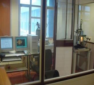
Few of the examples form results obtain using various modes are given below:
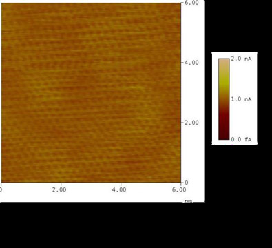
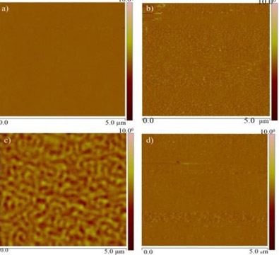
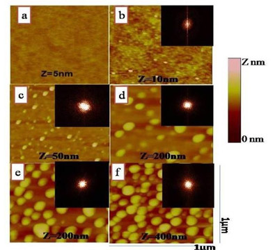
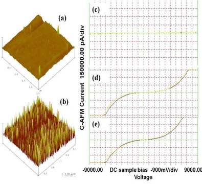
[1]. STM image of the single layer graphene flake deposited on Cu is shown in figure 1. [2]. Magnetic domains in (a) pristine Ni film and films annealed at 400 °C for (b) 60, (c) 90 and (d) 120 min. is observed using MFM mode as shown in ref [2]. [3]. Topographic evolution of 500keV Ar4+ ion beam irradiated InP(100) surfaces formation of self-organized In-rich nanodots was studied with tapping mode AFM as given in ref [3] [4]. The topographic (a) and current (b) image using C-AFM shows formation of conducting tracks in the sample after irradiation. The IV measurements show increased conductivity in samples with 5% (d) and 10% doping (e) as compared to unirradiated sample (c) as shown in ref [4].
[A Summary by Dr. P.K.Kulriya]
X-Ray Diffractometer (XRD) is the primary tool for investigating the structure of crystalline materials. An in-situ XRD facility has been setup in the materials science beam line of the superconducting LINAC accelerator. The advanced D-8 x-ray diffractometer (procured from Bruker AXS Germany) is funded by the IRHPA programme of Department of Science and Technology (DST), Govt. of India. A photograph of the in-situ XRD facility with its sample cooling unit is shown in the Figure 1. Generally, it has been observed that there are variations from sample to sample in the synthesis of nanoparticles and thin films, and the effect of ion irradiation critically depends on the initial state of the sample. Therefore, it becomes desirable that the ion fluence dependent study should be performed on the same sample. The in-situ XRD facility allows studying the structural modification in the same sample at the different ion fluence to understand the influence of swift heavy ion irradiation. Few materials exhibit phase transformation when they are irradiated with swift heavy ions at low temperature. To study such a system, liquid Helium based cryostat assembly is also integrated with in-situ XRD system. This setup is also used as a standard off-line diffractometer at low temperature and room temperature when there is no beam from the accelerator.
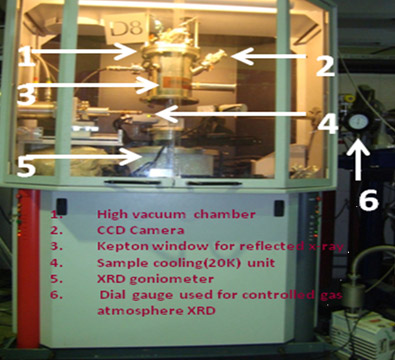
Normally, the XRD systems are consist of a vertically mounted goniometer with the sample in the horizontal plane. Since, the ion beam in IUAC LINAC accelerator is incident on the sample in the vertical plane, the samples mount needs to be vertical; therefore, the diffractometer is modified accordingly by manufacturer Bruker AXS Germany. A vacuum chamber is designed and fabricated to interface with the base of goniometer and the beamline. An adapter vacuum flange is inserted to couple the chamber with the base of a goniometer. This instrument equipped with a Cu Kα conventional x-ray source, Göbble mirror, LiF monochromator, scintillator detector. The facility is also equipped with a high speed position sensitive Vantec-1 detector besides conventional NaI(Tl) scintillation counter. It is about to 60 times faster as compared to scintillation counter with reasonably good resolution. This detector is very useful for in-situ ion irradiation experiments, where fast scanning is required to optimize the utilization of accelerator time. The detailed specifications of the instrument are given in the following reference “Setup for in-situ X-ray diffractometer study of swift heavy ion irradiated materials, P. K. Kulriya, F. Singh, A. Tripathi, R. Ahuja, A. Kothari, R. N. Dutt, Y. K. Mishra, Amit Kumar, D. K. Avasthi, Review of Scientific Instrument 78 (2007) 113901”. The XRD setup is used by many researchers for in-situ as well as offline XRD analysis. Following are the key references and highlights of the latest results from the in-situ XRD are given in the research section.
References
- Probing the temperature effects in the radiation stability of Nd2Zr2O7 pyrochlore under swift ion irradiation, Saurabh Kumar Sharma, V Grover, AK Tyagi, DK Avasthi, UB Singh, P K Kulriya, Materialia 6(2019) 100317.
- Probing swift heavy ion irradiation damage in Nd-doped zirconolite, Merry Gupta, P. K. Kulriya, R. C. Meena, S. Neumeier, S. S. Ghumman, Nucl. Instr. and Meth. B 453(2019)22-27
- Investigating the effect of material microstructure and irradiation temperature on the radiation tolerance of yttria stabilized zirconia against high energy heavy ions, Parswajit Kalita, Santanu Ghosh, Udai B Singh, Pawan K Kulriya, Vinita Grover, Rakesh Shukla, AK Tyagi, Gaël Sattonnay, Devesh K Avasthi, Journal of Applied Physics 125(2019) 115902.
- Structural response of Nd-stabilized zirconia and its composite under extreme conditions of swift heavy ion irradiation, Chiranjit Nandi, V Grover, P. K Kulriya, A. K. Poswal, Amrit Prakash, K. B. Khan, D. K. Avasthi, A. K. Tyagi, Journal of Nuclear Materials 499 (2018) 216-224
- Investigation of graphene oxide-hydrogen interaction using in-situ X-ray diffraction studies, Chetna Tyagi, P. K. Kulriya, Sunil Ojha, DK Avasthi, Ambuj Tripathi, International Journal of Hydrogen Energy 43(2018) 13339-13347
- Phase dependent radiation resistant behaviour of BaTiO3: An in‐situ X‐ray diffraction study, Renu Kumari, P K Kulriya, S Mishra, K Vasundhara, S N Achary, A K Tyagi, D K Avasthi, Journal of the American Ceramic Society (2017).
- In-situ high temperature irradiation setup for temperature dependent structural studies of materials under swift heavy ion irradiation, P K Kulriya, Renu Kumari, Rajesh Kumar; V Grover, R. Shukla, A K Tyagi, D K Avasthi, Nucl. Instr. and Meth. B 342(2015) 98.
- Enhanced Hydrogenation Properties of Size Selected Pd–C Core–Shell Nanoparticles; Effect of Carbon Shell Thickness, Vinod Singh, Bodh R. Mehta, Saurabh K. Sengar, Pawan K. Kulriya, Saif A. Khan, and Sonnada M. Shivaprasad, J. Phys. Chem. C, 2015, 119 (25), pp 14455–14460
- Micro-Raman study on the softening and stiffening of phonons in rutile titanium dioxide film: Competing effects of structural defects, crystallite size, and lattice strain, Subodh K Gautam, Fouran Singh, I Sulania, R. G Singh, P. K Kulriya, E Pippel, Journal of Applied Physics, 115 (2014) 143504.
- Temperature, pressure, and size dependence of Pd-H interaction in size selected Pd-Ag and Pd-Cu alloy nanoparticles: In-situ X-ray diffraction studies, Saurabh K Sengar, B. R Mehta, P. K. Kulriya, Journal of Applied Physics 115(2014) 114308.
- In-situ X-ray diffraction study of the growth of silver nanoparticles embedded in silica film by ion irradiation: The effect of volume fraction, Fouran Singh, Subodh K. Gautam, Pawan Kumar Kulriya, Jean Claude Pivin, Nucl. Instr. and Meth. B 311(2013)5.
- Enhanced hydrogenation and reduced lattice distortion in size selected Pd-Ag and Pd-Cu alloy nanoparticles, S K Sengar, B R Mehta, P K Kulriya, S A Khan, Applied Physics Letters 103, (2013)173107.
- Giant enhancement in ferromagnetic properties of Pd nanoparticle induced by intentionally created defects, P. K. Kulriya, B. R. Mehta, D. C. Agarwal, Praveen Kumar, S. M. Shivaprasad, J. C. Pivin, D. K. Avasthi, J. Appl. Phys. 112(2012) 014318
- Effect of grain size and microstructure on radiation stability of CeO2: an extensive study, V Grover, R Shukla, R Kumari, B P Mandal, P K Kulriya, S K Srivastava, S Ghosh, A K Tyagi, D K Avasthi Physical Chemistry Chemical Physics 16(2014) 27065-27073
- 200 MeV silver ion irradiation induced structural modification in YBa2Cu3O7-y thin films at 89 K: An in situ x-ray diffraction study, R. Biswal, J. John, P. Mallick, B. N. Dash, P. K. Kulriya, D. K. Avasthi, D. Kanjilal, D. Behera, T. Mohanty, P. Raychaudhuri, and N. C. Mishra, Journal of Applied Physics 106, 053912 (2009)
- Hydrogen induced lattice expansion and crystallinity degradation in palladium nanoparticles: Effect of hydrogen concentration, pressure, and temperature, Manika Khanuja, B. R. Mehta, Pragya Agar, P. K. Kulriya, and D. K. Avasthi, J. Appl. Phys. 106 (2009) 093515
- Controlled growth of gold nanoparticles induced by ion irradiation: An in situ x-ray diffraction study, Y. K. Mishra, D. K. Avasthi, P. K. Kulriya, F. Singh, D. Kabiraj, and A. Tripathi, J. C. Pivin, I. S. Bayer and A. Biswas, Appl. Phys. Lett., 90 (2007) 073110
- Setup for insitu X-ray diffractometer study of swift heavy ion irradiated materials, P. K. Kulriya, F. Singh, A. Tripathi, R. Ahuja, A. Kothari, R. N. Dutt, Y. K. Mishra, Amit Kumar, D. K. Avasthi, Review of Scientific Instrument 78 (2007) 113901
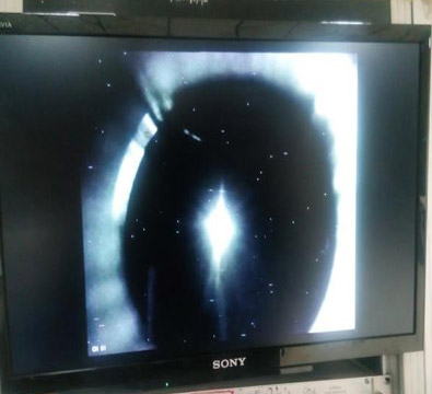
It is well known that when an ion beam with energy of a few MeV/u impacts on a crystalline or organic specimen, visible light is often observed. This light induced by the energetic ions is termed as Ionoluminescence. IL spectroscopy is a very useful method for understanding material phenomena such as ion matter interaction, impurity characterization, and local symmetry studies. IL can be used not only for characterizing the materials; it can be applied during material modification with ion beams in order to follow the creation of intrinsic defects. Most of the work is planned in view of the applications like new optoelectronic devices, Optical telecommunication, Flat displays (TLD, LCD, LED, ELD) CRT, White LED’s, Lamps & Displays etc.
- Kumar, M., Rajput, P., Singh, P.K., Yadav, A.C., Pradhan, S.L., Baranwal, V., Singh, U.B., Jha, S.N., Singh, F., Luminescence properties of BaMgAl10O17: Mn2+ nanophosphors, (2019) Journal of Alloys and Compounds, 799, pp. 556-562.
- Satyanarayana Reddy, S., Nagabhushana, K.R., Singh, F., Structure and crystal field analysis using ionoluminescence of Al2O3: Tm3+ phosphor, (2019) Journal of Luminescence, 214, art. no. 116553.
- Shivaramu, N.J., Nagabhushana, K.R., Lakshminarasappa, B.N., Singh, F., Ion beam induced luminescence studies of sol gel derived Y2O3:Dy3+ nanophosphors, (2016) Journal of Luminescence, 169, pp. 627-634.
- Kumar, M., Rajput, P., Singh, P.K., Yadav, A.C., Khan, S.A., Jha, S.N., Singh, F., Pandey, A.C., Europium activated gadolinium sulfide nanoparticles, (2016) RSC Advances, 6 (110), pp. 108523-108529.
- Premkumar, H.B., Sunitha, D.V., Nagabhushana, H., Sharma, S.C., Prashantha, S.C., Singh, F., Nagabhushana, B.M., Zhao, G., Chen, J., Chakradhar, R.P.S., Heavy ion induced luminescence studies of YAlO3: Tb3+, Tm3+ single crystals, (2014) Materials Research Express, 1 (1), art. no. 015908.
- Sunitha, D.V., Nagabhushana, H., Sharma, S.C., Singh, F., Nagabhushana, B.M., Dhananjaya, N., Shivakumara, C., Chakradhar, R.P.S., Structural, iono and thermoluminescence properties of heavy ion (100 MeV Si7+) bombarded Zn2SiO4:Sm3+ nanophosphor, (2013) Journal of Luminescence, 143, pp. 409-417.
- Prashantha, S.C., Lakshminarasappa, B.N., Singh, F. 100 MeV Si 8 ion induced luminescence and thermoluminescence of nanocrystalline Mg 2SiO 4:Eu3 (2012) Journal of Luminescence, 132 (11), pp. 3093-3097.
- Premkumar, H.B., Sunitha, D.V., Singh, F., Nagabhushana, H., Sharma, S.C., Nagabhushana, B.M., Zhao, G., Chen, J., Chakradhar, R.P.S., Luminescence and defect studies of YAlO 3:Dy 3+, Sm 3+ single crystals exposed to 100 MeV Si 7+ ion beam, (2012) Journal of Luminescence, 132 (10), pp. 2679-2683.
- Sunitha, D.V., Nagabhushana, H., Singh, F., Nagabhushana, B.M., Sharma, S.C., Chakradhar, R.P.S., Thermo, Iono and photoluminescence properties of 100 MeV Si 7 ions bombarded CaSiO3:Eu3+ nanophosphor, (2012) Journal of Luminescence, 132 (8), pp. 2065-2071
- Nagabhushana, H., Singh, F., Sharma, S.C., Nagabhushana, B.M., Chakradhar, R.P.S., Ionoluminescence studies of natural kyanite mineral from different parts of Indian origin, (2012) Spectrochimica Acta - Part A: Molecular and Biomolecular Spectroscopy, 86, pp. 15-19.
- Sunitha, D.V., Nagabhushana, H., Singh, F., Sharma, S.C., Dhananjaya, N., Nagabhushana, B.M., Chakradhar, R.P.S., Ion beam induced amorphization and bond breaking in Zn 2 SiO 4 :Eu 3+ nanocrystalline phosphor, (2012) Spectrochimica Acta - Part A: Molecular and Biomolecular Spectroscopy, 90, pp. 18-21.
- Sunitha, D.V., Nagabhushana, H., Singh, F., Dhananjaya, N., Sharma, S.C., Nagabhushana, B.M., Shivakumara, C., Chakradhar, R.P.S., Swift heavy ion induced structural, iono and photoluminescence properties of β-CaSiO 3:Dy 3+ nanophosphor, (2012) Spectrochimica Acta - Part A: Molecular and Biomolecular Spectroscopy, 93, pp. 300-305.
- Lakshminarasappa, B.N., Prashantha, S.C., Singh, F. Ionoluminescence studies of combustion synthesized Dy3+ doped nano crystalline forsterite (2011) Current Applied Physics, 11 (6), pp. 1274-1277.
- Vij, A., Kumar, R., Singh, F., Singh, N., 120 MeV Ag9+ ions induced ionoluminescence of SrS:Ce (2011) AIP Conference Proceedings, 1349 (PART A), pp. 491-492.
- Nagabhushana, H., Umesh, B., Nagabhushana, B.M., Lakshminarasappa, B.N., Singh, F., Chakradhar, R.P.S., Determination of the chemical states of impurities in natural kyanite by the ionoluminescence technique, (2009) Philosophical Magazine, 89 (11), pp. 995-1004.
- Nagabhushana, H., Prashantha, S.C., Lakshminarasappa, B.N., Singh, F., Ionoluminescence and photoluminescence studies of Ag8+ ion irradiated kyanite, (2008) Journal of Luminescence, 128 (1), pp. 7-10.
- Nagabhushana, H., Prashantha, S.C., Nagabhushana, B.M., Lakshminarasappa, B.N., Singh, F., Chakradhar, R.P.S., Ion beam-induced luminescence and photoluminescence of 100 MeV Si8+ ion irradiated kyanite single crystals, (2008) Solid State Communications, 147 (9-10), pp. 377-380.
- Nagabhushana, H., Lakshminarasappa, B.N., Singh, F., Avasthi, D.K., Ionoluminescence and photoluminescence in swift heavy ion-irradiated Al2SiO5, (2003) Radiation Measurements, 36 (1-6 SPEC.), pp. 643-646.
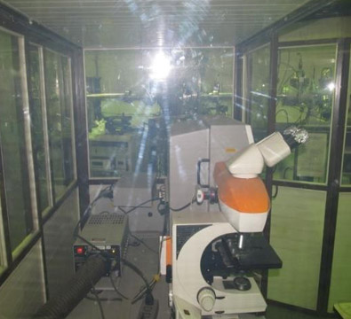
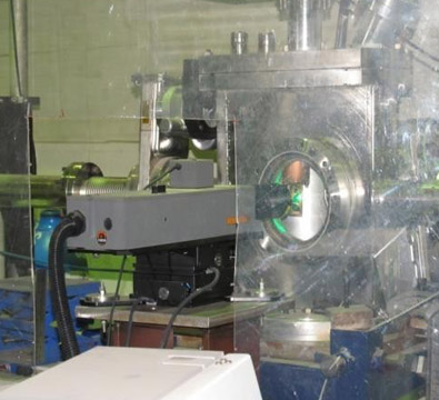
Raman spectroscopy is technique is based on inelastic scattering of monochromatic light by matter and is capable of probing the structure of gases, liquid and solids. Raman scattering is only possible from Raman active material which depends on symmetry-allowed Raman active vibrational modes of solids. Raman measurements can provide information about the strength of inter-atomic and intermolecular bonds, the mechanical strain in a solid, the composition of multi component matter, the degree of crystallinity and the effects of pressure and temperature on phase transformations. We have In-Via micro-Raman microscope from Renishaw consist Argon ion laser 514.5 nm (TEM00) photons of 50 mW power, CCD detector and magnification lenses., which can be utilized during ex-situ and in-situ measurements according to requirements of the users. The facility located in Beam Hall 2 nearby XRD and NAND at IUAC, which is attached to the beam line. This facility is capable for energetic ion irradiation at room temperature as well as liquid nitrogen temperature with in-situ measurement of irradiated thin films and powdered materials. The Fiber-Optic Probe (FOP) is integrated with high vacuum chamber at 900 with respect to beam direction. The demonstration of the ex-situ and in-situ facility is shown by figure below.
Selected Publications of Raman
- “Micro-Raman investigations on zirconium oxide film during swift heavy ion irradiation to study crystalline-to-crystalline phase transformation kinetics by cascade overlap model.” Fouran Singh, Mukesh Rawat, Subodh K. Gautam, Sunil Ojha: Journal of Applied Physics 126 (2019) 025901.
- “High temperature mediated rocksalt to wurtzite phase transformation in cadmium oxide nano-sheets and its theoretical evidence.” Arkaprava Das, Chetan Prakash Saini, Deobrat Singh, Rajeev Ahuja, Anumeet Kaur, Sergei Aliukov, D. K. Shukla, Fouran Singh: Nanoscale 11 (2019) 14802.
- “Stiffening of phonons with enhanced hybridization and structural phase transformation upon Pr-doping in BiFeO3.” Priyanka Trivedi, Fouran Singh, Brinda Vyas, Hetal Kundalia, D.K. Shukla, Sudhindra Rayaprol, D.G. Kuberkar, Physica B 571 (2019) 247.
- “Evolution of symmetry forbidden and silent Raman modes of cadmium doped zinc oxide films activated by swift heavy ion irradiation.” Naina Gautam, Himanshi Gupta, A. Kapoor, Fouran Singh, Physica B 570 (2019) 13.
- “In Situ Study of Radiation Stability and Associated Conduction Mechanisms of Nb-Doped TiO₂/p-Si Heterojunction Diode Under Swift Heavy Ion Irradiation.” Subodh Kumar Gautam, Jitendra Singh, Ram Gopal Singh, Naina Gautam, Priyanka Trivedi, Fouran Singh: IEEE Transactions on Electron Devices 66 (2019) 1475.
- “Multifunctional hybrid diode: Study of photoresponse, high responsivity, and charge injection mechanisms” J Singh, RG Singh, SK Gautam, Fouran Singh, Journal of Applied Physics 123 (17), 174503 2018.
- “Reversible phase transformation phenomenon in titanium dioxide films: Evidence beyond interface-nucleation and dissolution-precipitation kinetics” SK Gautam, J Singh, DK Shukla, E Pippel, P Poddar, Fouran Singh, Acta Materialia 146, 253-264 2018.
- “Highly selective and reversible NO2 gas sensor using vertically aligned MoS2 flake networks” R Kumar, PK Kulriya, M Mishra, Fouran Singh, G Gupta, M Kumar, Nanotechnology 29 (46), 464001 2018.
- Electronic excitation induced anomalous band gap enhancement in Ni x Cd 1-x O thin films. Arkaprava Das, Fouran Singh: Vacuum 146 (2017) 287.
- “Virtual gap states induced modifications in charge neutrality level in cadmium oxide thin films.” Arkaprava Das, Subodh Gautam, G.R. Umapathy, Sunil Ojha, Fouran Singh: Materials Research Express 4 (2017) 45901.
- “The role of ion irradiation in activating silent Raman modes via tuning in plasmonic behaviour and surface disorder of Au/ZnO/Pt NFG system.” Udai B. Singh, Subodh K. Gautam, Sunil Kumar, Sunil Ojha, Santanu Ghosh, Fouran Singh: EPL (Europhysics Letters) 119 (2017) 66002.
- “Study of phase transformation induced by electronic excitation in pure and yttrium doped ZrO2 thin films.” R C Ramola, Mukesh Rawat, Kanchan Joshi, Arkaprava Das, Subodh K Gautam, Fouran Singh: Materials Research Express 4 (2017) 096401.
- “Band gap widening and narrowing in Cu-doped ZnO thin films,” K. Joshi, M. Rawat, S.K. Gautam, R.G. Singh, R.C. Ramola, Fouran Singh, Journal of Alloys and Compounds 680 (2016) 252.
- “Swift heavy ion induced structural phase generation and enhanced luminescence from CdS based nanocomposites,” P. Kumar, N. Saxena, Fouran Singh, V. Gupta, Surface and Coatings Technology 306 (2016) 305.
- “Micro-Raman and electronic structure study on kinetics of electronic excitations induced monoclinic-to-tetragonal phase transition in zirconium oxide films,” M. Rawat, A. Das, D.K. Shukla, P. Rajput, A. Chettah, D.M. Phase, R.C. Ramola, Fouran Singh, RSC Advances 6 (2016) 104425.
- “Electronic structure modification and Fermi level shifting in niobium-doped anatase titanium dioxide thin films: A comparative study of NEXAFS, work function and stiffening of phonons,” S.K. Gautam, A. Das, S. Ojha, D.K. Shukla, D.M. Phase, Fouran Singh, Physical Chemistry Chemical Physics 18 (2016) 3618.
- “Carrier transport mechanism of highly-sensitive niobium doped titanium dioxide/p-Si heterojunction photodiode under illuminations by solar simulated light,” S.K. Gautam, A. Das, R.G. Singh, V.V.S. Kumar, Fouran Singh, Journal of Applied Physics 120 (2016) 214502.
- “Correlations of charge neutrality level with electronic structure and p-d hybridization,” A. Das, S.K. Gautam, D.K. Shukla, Fouran Singh, Scientific Reports 7 (2017) 40843.
- “Growth of highly transparent CdxZn1-xO (CZO) thin films: Structural and optical studies” Naina Gautam, Fouran Singh, Subodh K. Gautam, R.G. Singh, S. Ojha, A. Kapoor, Journal of Alloys and Compounds 650 (2015) 311-317.
- “Anomalous behavior of B1g mode in highly transparent anatase nano-crystalline Nb-doped Titanium Dioxide (NTO) thin films” Subodh K. Gautam, Naina Gautam, R. G. Singh, S. Ojha, D. K. Shukla, and Fouran Singh, AIP Advances 5 (2015) 127212-13.
- “Composition dependent Fermi level shifting of Au decorated MoS2 nanosheets” Jyoti Shakya, Arun Singh Patel, Fouran Singh, and Tanuja Mohanty, Appl. Phys. Lett. 108 (2016) 013103-4.
- “Giant enhancement of the n-type conductivity in single phase p-type ZnO:N thin films by intentionally created defect clusters and pairs” Subodh K. Gautam, R.G. Singh, V.V. Siva Kumar, Fouran Singh, Solid State Communications 218 (2015) 20.
- “Defect controlled ferromagnetism in xenon ion irradiated zinc oxide”, P Satyarthi, S Ghosh, P Mishra, BR Sekhar, Fouran Singh, P Kumar, D Kanjilal, RS Dhaka, P Srivastava, Journal of Magnetism and Magnetic Materials, 385 (2015) 318.
- “Micro-Raman study on the softening and stiffening of phonons in rutile titanium dioxide film: competing effects of structural defects, crystallite size, and lattice strain” Subodh K. Gautam, Fouran Singh, I. Sulania,1 R. G. Singh, P. K. Kulriya, and E. Pippel, J. Appl. Phys. 115, 143504 (2014).
- “Purification/annealing of graphene with 100-MeV Ag ion irradiation” Sunil Kumar, Ambuj Tripathi, Fouran Singh, Saif Ahmad Khan, Vikas Baranwal, Devesh Kumar Avasthi, Nanoscale research letters, 9 (2014) 126.
- “Correlation between surface phonon mode and luminescence in nanocrystalline CdS thin films: An effect of ion beam irradiation”, P. Kumar, N. Saxena, V. Gupta, Fouran Singh, A. Agarwal, Journal of Applied Physics 116 (2014) 043517.
- Radiation stability of graphene under extreme conditions S Kumar, A Tripathi, SA Khan, C Pannu, DK Avasthi, Applied Physics Letters 105 (2014), 133107.
- “Influence of thermal annealing and ion irradiation on zinc silicate phases in nanocomposite ZnO–SiOx thin films”, V.S.K. Valiveti, Fouran Singh, S. Ojha, D. Kanjilal, Applied Surface Science 317 (2014) 1075.
- “Disorder induced semiconductor to metal transition and grain boundary modifications in nanocrystalline zinc oxide thin film”, Fouran Singh, Babloo Chaudhary, Vinod Kumar, R. G. Singh, Sanjeev Kumar and A. Kapoor, J. Appl. Phys. 112 (2012) 073101.
- “Softening of phonons by lattice defects and structural strain in heavy ion irradiated nanocrystalline zinc oxide films”, Fouran Singh, R. G. Singh, Vinod Kumar, S. A. Khan, and J. C. Pivin, J. Appl. Phys. 110 (2011) 083520.
- “Origin of swift heavy ion induced stress in textured ZnO thin films: An in situ X-ray diffraction study” Fouran Singh, P.K. Kulriya and J.C. Pivin, Solid State Communications 150 (2010) 1751.
- “Electronic excitation induced tuning of surface plasmon resonance of Ag nanoparticles in fullerene C70 matrix” R. Singhal, D C Agarwal, Y K Mishra, Fouran Singh, J C Pivin, R Chandra, D K Avasthi, J. Phys. D: Appl. Phys. 42 (2009) 155103.
- “Modifications of structural, optical and electrical properties of nanocrystalline bismuth sulphide by using swift heavy ions” R.R. Ahire, Abhay A. Sagade, S.D. Chavhan, V. Huse, Y.G. Gudage, Fouran Singh, D.K. Avasthi, D.M. Phase, Ramphal Sharma, Current Applied Physics 9 (2009) 374-379.
- “Synthesis and characterization of silver-fullerene C70 nanocomposite”, R. Singhal, D.C. Agarwal, S. Mohapatra, Y.K. Mishra, D. Kabiraj, Fouran Singh, D.K. Avasthi et al, Appl. Phys. Lett. 93, 103114 (2008).
- “On the origin of photoluminescence in indium oxide octahedron structures” Mukesh Kumar, V. N. Singh, Fouran Singh, K. V. Lakshmi, B. R. Mehta, and J. P. Singh, Appl. Phys. Lett. 92, 171907 (2008).
- “Conducting carbon nanopatterns (nanowire) by energetic ion irradiation” Amit Kumar, Fouran Singh, A Tripathi, Julien Pernot, J C Pivin and D K Avasthi, J. Phys. D: Appl. Phys. 41 (2008) 095304.
- “Studies on high electronic energy deposition in transparent conducting indium tin oxide thin films” N G Deshpande, Y G Gudage, A Ghosh, J C Vyas, Fouran Singh, A Tripathi and Ramphal Sharma,J. Phys. D: Appl. Phys. 41 (2008) 035308.
- “Synthesis of confined electrically conducting carbon nanowires by heavy ion irradiation of fullerene thin film” Amit Kumar, D. K. Avasthi, A. Tripathi, D. Kabiraj, Fouran Singh and J. C. Pivin J. Appl. Phys. 101 (2007) 014308.
- “Fabrication of carbon nanostructures (nanodots, nanowires) by energetic ion irradiation” A. Kumar, D.K. Avasthi, Fouran Singh, J. C. Pivin, A. Tripathi J. Phys. D: Appl. Phys. 40 (2007) 2083-2088.
- “Engineering of nanocrystalline cadmium sulfide thin films by using swift heavy ions” R R Ahire, Abhay A Sagade, N G Deshpande, S D Chavhan, Ramphal Sharma and Fouran Singh, J. Phys. D: Appl. Phys. 40 (2007) 4850-4854.
- “Electrical transport study of structural phase transitions in C60 films and the effect of swift heavy ion irradiation” Amit Kumar, Fouran Singh, Ravi Kumar, A. Tripathi, D.K. Avasthi and J.C. Pivin Solid State Communications 138 (2006) 448.
- “Synthesis and characterization of ZnO thin film grown by electron beam evaporation” D.C. Agarwal, R.S. Chauhan, Amit Kumar, D. Kabiraj, Fouran Singh, S.A. Khan, D.K. Avasthi, J.C. Pivin, M. Kumar, J. Ghatak, and P.V. Satyam J. Appl. Phys. 99 (2006) 123105.
- Radiation stability of graphene under extreme conditions S Kumar, A Tripathi, SA Khan, C Pannu, DK Avasthi, Applied Physics Letters 105 (2014), 133107.
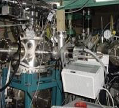
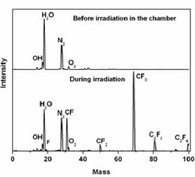
The Pfeiffer QMA 422 quadrupole mass analyzer system with SIMS option (under IRHPA programme of DST) operating at 2.25 MHz and can mass analyze in the range 1-1024 amu with mass separation (ΔM/M) better than 0.01 is installed in materials science beamline. The QMA has a 3 lens optics The facility is used for on line detection of release of gases, specially from polymers and online study of electronic sputtering. The QMS is attached to a 90° port of ultra-high vacuum (UHV) chamber. The probe consisting of 3 lens optics for detecting both positive and negative ions as well as neutral atoms is nearly 5 mm from the sample surface during the measurements.
Recent Publications:
- G. B. V. S. Lakshmi, Jai Prakash, S. A. Khan, Azher M. Siddiqui, and M. Zulfequar, Modifications induced by swift heavy ion beam of 60 MeV Si5+ in Poly(3-octylthiophene), Science of Advanced Materials 4 (2012) 1024-1030.
- K. Sangeetha, R. Ramesh Babu, K. Ramamurthi, Jai Prakash, and S. A. Khan, Spectral studies on Ag8+ions irradiated LAHCl.H2O and LAHBr.H2O single crystals, Spectrochemica Acta Part A 79 (2011) 884-888.
- G. B. V. S. Lakshmi, D. K. Avasthi, Jai Prakash, Azher M. Siddiqui, Vazid Ali, S. A. Khan, and M. Zulfequar, Structural, optical and gas evolution studies of 60 MeV Si5+ ion irradiated PoT-PVC blends, Adv. Mat. Lett. 2(2) (2011) 125-130
- Jai Prakash, A. Tripathi, S. A. Khan, J. C. Pivin, F. Singh, Jalaj Tripathi, Sarvesh Kumar, and D. K. Avasthi, Ion beam induced interface mixing of Ni on PTFE bilayer system studied by quadrupole mass analysis and electron spectroscopy for chemical analysis, Vacuum 84(11) (2010) 1275-1279.
Ramcharan Meena, and K. Asokan
In the transport lab, the following measurements are being done and a brief detail alongwith selected recent published papers are given..
- Resistivity Measurement: The room temperature resistance value and expected behavior of resistance with temperature decides that the measurement mode to be used: two or four probe. To find the resistivity behavior with temperature for the low resistive samples, the method used is four probe method. It is done with the help of Keithley Source meter (Model No. 2612B) or delta mode (Keithley current source (6221), Keithely Nanovoltmeter (2182A)) and Lakeshore temperature controller (Model no-340). For high resistive samples to find the resistivity behavior with temperature we use Keithley Electrometer (Model No. 6517B) and same temperature controller. The measurement range in resistance is (𝜇Ω−𝐺𝛺) and temperature range is (10K-450K). The temperature is measured by using diode or Pt-100 sensor and temperature is varied by cartridge heater. The vacuum during the measurement is of the order of 10-3 mbar. Temperature during these experiments is in millikelvin.
Some recent Publications
- Enhancement of thermoelectric performance of n-type In2(Te0.94Se0.06)3 thin films by electronic excitations, Pandian Mannu, Matheswaran Palanisamy, Gokul Bangaru, Sathyamoorthy Ramakrishnan, Ramcharan Meena, Chung-Li Dong, and Asokan K. Applied Surface Science 505 (2020) 144115.
- Investigations on magnetic and electrical properties of Zn doped Fe2O3 nanoparticles and their correlation with local electronic structures, Parmod Kumar, Vikas Sharma, Jitendra P. Singh, Ashish Kumar, Surjeet Chahal, K. Sachdev, K.H. Chae, Ashok Kumar, K. Asokan and D. Kanjilal. Journal of Magnetism and Magnetic Materials 489 (2019) 165398.
- Tuning the electrical and thermoelectric properties of N ion implanted SrTiO3 thin films and their conduction Mechanisms, Anuradha Bhogra, Anha Masarrat, Ramcharan Meena, Dilruba Hasina, Manju Bala,Chung-Li Dong, Chi-Liang Chen, Tapobrata Som, Ashish Kumar & Asokan Kandasami. Scientific Reports (2019) 9:14486
- Studies on transport properties of manganite based nano-micro particles-matrix composites, Hardik Gohil, Hetal Boricha, K.N. Rathod, Keval Gadani, Bhargav Rajyaguru, A.D. Joshi, D.D. Pandya, K. Asokan, N.A. Shah, P.S. Solanki. Journal of Alloys and Compounds 775 (2019) 1016-1027
- Effect of Fe ion implantation on the thermoelectric properties and electronic structures of CoSb3 thin films, Anha Masarrat, Anuradha Bhogra, Ramcharan Meena, Manju Bala, Ranveer Singh,Vineet Barwal, Chung-Li Dong, Chi-Liang Chen, T. Som, Ashish Kumar, A. Niazi and K. Asokan. RSC Adv., 2019, 9, 36113.
- Tuning of the Thermoelectric Properties of Bi2Te3 Nanorods Using Helium Ion Irradiation, Sinduja M, S. Amirthapandian, P. Magudapathy, S. K. Srivastava, and K. Asokan. ACS Omega 2018, 3, 18411−18419.
- Hall Effect: The Hall effect measurement helps to determine the type of charge carrier present in the semiconducting material. It is done with the help of Ecopia Hall effect system (Model No.HMS-3000). The magnetic field during the measurement is 0.57Tesla. Before going for the Hall Effect experiment, linearity of all the contacts is need to be checked by doing the I-V measurement. By this experiment we can get various parameters of semiconducting materials like carrier concentration, mobility, type of charge carrier, conductivity, and magneto-resistance. These measurement can be done at two temperatures room temperature and liquid nitrogen temperature.
Some recent Publications
- 200 MeV Ag15+ swift heavy ion beam induced property modifications in Nb2O5 thin films by fluence variation, R. Rathika, M. Kovendhanb, D. Paul Joseph, K. Vijayarangamuthu, A. Sendil Kumar, C. Venkateswaran, K. Asokan, S. Johnson Jeyakumar. Journal of Physics and Chemistry of Solids 135 (2019) 109089.
- 200 MeV Ag15+ ion beam irradiation induced modifications in spray deposited MoO3 thin films by fluence variation, R. Rathika, M. Kovendhan, D. Paul Joseph, K. Vijayarangamuthu, A. Sendil Kumar, Venkateswaran, K. Asokan, S. Johnson Jeyakumar. Nuclear Engineering and Technology 51 (2019) 1983-1990.
- Effect of 200 MeV Ag15+ ion beam irradiation at different fluences on WO3 thin films, R. Rathika, M. Kovendhanb, D. Paul Joseph, A. Sendil Kumar, K. Vijayarangamuthu, C. Venkateswaran, K. Asokan and S. Johnson Jeyakumar. Nuclear Inst. and Methods in Physics Research B 439 (2019) 51–58.
- Seebeck coefficient measurement: It is measured with the help of differential method. With this setup, Seebeck coefficient of two samples can be measured simultaneously.
To measure the Seebeck coefficient we use Keithley current source ((Model No. 6221)-to create the temperature difference across the material by joule heating), Keithely Nanovoltmeter ((Model No. 2182A)- to read the Seebeck coefficient of one sample and read the temperature difference by differential thermocouple), Agilent Nanovoltmeter ((Model No.34420 A)- to read the Seebeck coefficient of second sample) and Lakeshore temperature controller (Model No-336) to vary the base temperature of the sample. The base temperature can be varied from 100K to 500K and measured with the help of Pt-100 sensor. During Seebeck coefficient measurements all the instruments are connected by Lab view software for accurate and fast measurement.
Some recent Publications
- Investigations on morphology and thermoelectric transport properties of Cu ion implanted bismuth telluride thin film, Sinduja M., S. Amirthapandian, Anha Masarratb, R. Krishnan, S.K. Srivastava, Asokan Kandasami. Thin Solid Films 697 (2020) 137834.
- Enhancement of thermoelectric performance of n-type In2(Te0.94Se0.06)3 thin films by electronic excitations, Pandian Mannu, Matheswaran Palanisamy, Gokul Bangaru, Sathyamoorthy Ramakrishnan, Ramcharan Meena, Chung-Li Dong, and Asokan Kandasami. Applied Surface Science 505 (2020) 144115.
- Tuning the electrical and thermoelectric properties of N ion implanted SrTiO3 thin films and their conduction Mechanisms, Anuradha Bhogra, Anha Masarrat, Ramcharan Meena, Dilruba Hasina, Manju Bala,Chung-Li Dong, Chi-Liang Chen, Tapobrata Som, Ashish Kumar & Asokan Kandasami. Scientific Reports (2019) 9:14486.
- Effect of Fe ion implantation on the thermoelectric properties and electronic structures of CoSb3 thin films, Anha Masarrat, Anuradha Bhogra, Ramcharan Meena, Manju Bala, Ranveer Singh,Vineet Barwal, Chung-Li Dong, Chi-Liang Chen, T. Som, Ashish Kumar, A. Niazi and K. Asokan. RSC Adv., 2019, 9, 36113.
- Structure and transport properties of Ni implanted CoSb3 skutterudite thin films synthesized via pulse laser deposition, Manju Bala, Anha Masarrat, Anuradha Bhogra, Ramcharan Meena, Ying-Rui Lu, Yu Cheng Huang, Chi Liang Chen, Chung Li Dong, Sunil Ojha, Devesh Avasthi, Subramanian Annapoorni, and Kandasami Asokan. ACS Appl. Energy Mater. 2018, 1, 11, 5879-5886.
- I-V, C-V Measurement: To characterize the semiconductor device like diode, transistor can be done with the help of Agilent Semiconductor Device Analyzer (Model No-B1500A). One can do various measurements like I-V, Pulsed I-V, Transient I-V, C-V (frequency range 1 kHz to 1 MHz and voltage range is mV to V). Most of the measurements are done at room temperature with the help of pressure probes. The pressure probes are made up of W metal. It is the device having the both source meter and capacitance meter.
Semiconductor device analyzer is mostly used for the semiconducting samples only, to do the I-V measurements of insulating samples we used Keithley Electrometer (Model No. 6517B) can be used to measure the current up to the range of pA. Same pressure probes mentioned above are used to make the contact with the sample. To hold the sample at particular position vacuum chuck is used. To change the contact position, pressure probes position can be changed by the screws.
Some recent Publications
- Investigations on morphology and thermoelectric transport properties of Cu ion implanted bismuth telluride thin film, Sinduja M., S. Amirthapandian, Anha Masarratb, R. Krishnan, S.K. Srivastava, Asokan Kandasami. Thin Solid Films 697 (2020) 137834.
- Enhancement of thermoelectric performance of n-type In2(Te0.94Se0.06)3 thin films by electronic excitations, Pandian Mannu, Matheswaran Palanisamy, Gokul Bangaru, Sathyamoorthy Ramakrishnan, Ramcharan Meena, Chung-Li Dong, and Asokan Kandasami. Applied Surface Science 505 (2020) 144115.
- Tuning the electrical and thermoelectric properties of N ion implanted SrTiO3 thin films and their conduction Mechanisms, Anuradha Bhogra, Anha Masarrat, Ramcharan Meena, Dilruba Hasina, Manju Bala,Chung-Li Dong, Chi-Liang Chen, Tapobrata Som, Ashish Kumar & Asokan Kandasami. Scientific Reports (2019) 9:14486.
- Effect of gamma irradiation on structure and photoconductivity of amorphous Sb30Se70 chalcogenide films, Shaveta Sharma, Rita Sharma, Praveen Kumar, R. Thangaraj, K. Asokan, M. Mian. Journal of Non-Crystalline Solids 530 (2020) 119807.
- Medium Energy Carbon and Nitrogen Ion Beam Induced Modifications in Charge Transport, Structural and Optical Properties of Ni/Pd/n-GaN Schottky Barrier Diodes, Santosh Kumar, Xiang Zhang, Vinay Kumar Mariswamy, Varra Rajagopal Reddy, Asokan Kandasami, Arun Nimmala, S.V.S Nageswara Rao, Jue Tang, Seeram Ramakrishnna and Krishnaveni Sannathammegowda. Materials 2020, 13, 1299.
- Thermionic emission driven resistive switching behaviour in Ca and Sr doped YMnO3 thin film devices, Manan Gal, Keval Gadani, Davit Dhruv, Zalak Joshi, Alpa Zankat, Bhargav Rajyaguru, A. D. Joshi , K. Asokan , P.S. Solanki , N.A. Shah. Solid State Communications 303-304 (2019) 113737.
- Influence of barrier inhomogeneities on transport properties of Pt/MoS2 Schottky barrier junction, Neetika, Sandeep Kumar, Amit Sanger, Hemant K. Chourasiya, Ashish Kumar,K. Asokan, Ramesh Chandra and V.K. Malik. Journal of Alloys and Compounds 797 (2019) 582-588.
- Defect dynamics in the resistive switching characteristics of Y0.95Sr0.05MnO3 films induced by electronic excitations, Keval Gadani, K.N. Rathod, Davit Dhruv, Hetal Boricha, Khushal Sagapariya,A.D. Joshi, D.D.
- Dielectric Measurement: It is done with the help of Agilent LCR meter. (Model No E4980A) and Lakeshore temperature controller (Model no-340). One can determine various parameters like capacitance, inductance, impedance, dissipation factor, quality factor, phase angle, direct current-voltage with this measurement. It can be done for both type of samples (bulk, thin film), the method used in the capacitance method. The measurement range in frequency is (20 Hz-2MHz) and temperature range is (10K-450K). It can be done by varying both parameters (a) temperatures (keeping frequency fixed) and (b) frequency (keeping temperature fixed). The temperature is measured by diode or Pt-100 sensor and temperature is varied by cartridge heater. The vacuum during the measurement is of the order of 10-3 mbar.
Some recent Publications
- Effect of La-doping on dielectric properties and energy storage density of lead-free Ba(Ti0.95Sn0.05)O3 ceramics, R. Kumar, I. Singh, R. Meena, K. Asokan, Balaji Birajdar, S. Patnaik. Materials Research Bulletin 123 (2020) 110694.
- Investigations on magnetic and electrical properties of Zn doped Fe2O3 nanoparticles and their correlation with local electronic structures, Parmod Kumara, Vikas Sharma, Jitendra P. Singh, Ashish Kumar, Surjeet Chahal, K. Sachdev, K.H. Chae, Ashok Kumar, K. Asokand, and D. Kanjilal. Journal of Magnetism and Magnetic Materials 489 (2019) 165398.
- Temperature-dependent AC conductivity and dielectric and impedance properties of ternary In–Te–Se nanocomposite thin films, Pandian Mannu, Matheswaran Palanisamy,Gokul Bangaru, Sathyamoorthy Ramakrishnan, Asokan Kandasami, Pawan Kumar. Applied Physics A (2019) 125:458
- Electrical behavior and structure – property correlations in La1–xPrxMnO3 (0 ≤ x ≤ 1) ceramics, Bhagyashree Udeshi, Hetal Boricha, Bhargav Rajyaguru, Keval Gadani, K.N. Rathod, Davit Dhruv, S.B. Kansara, R.K. Trivedi, D.D. Pandya, K. Asokan, P.S. Solanki and N.A. Shah. Ceramics International 45 (2019) 1098–1109.
- In-situ Transport Measurement: To see the property of the material or device with ion irradiation, we do the in-situ measurements. By this technique one can avoid sample to sample variation and more no of studies can be done on a single sample. For in-situ device characterization, the Agilent Semiconductor Device Analyzer (Model No-B1500A) is used and for other type of samples source meter or electrometer can also be used. Various in-situ transport facilities are I-V, C-V, Resistivity, DLTS, etc. The in-situ measurements are done at room temperature as well as variable temperature range 100K-500K. During in-situ measurements sample in the vacuum which is of the order of 10-7 mbar and all the instruments are connected by Lab view software for accurate and fast measurement.
Some recent Publications
- Radiation stability and reliability of Cu–ZnO/P3OT hybrid heterostructures under swift heavy ion irradiations, Jitendra Singh, Himanshi Gupta, A. Kumar, R.G. Singh and Fouran Singh. Materials Science in Semiconductor Processing 108 (2020) 104885.
- Study of ZnO/NiO heterojunction I-V characteristics measured in-situ during 200 MeV Ag ion irradiation, P.K. Das, R. Biswal, R.J. Choudhary, S.A.Khan, R.C. Meena, N.C. Mishra and P. Mallick. Materials Research Express 6 (2019) 106413.
- Swift heavy ions-induced degradation on the electrical characteristics of silicon NPN power transistors, T. M. Pradeep, Vinayakaprasanna N. Hegde, N. Pushpa, Ambuj Tripathi, K. Asokan and A. P. Gnana Prakash. Radiation Effects and Defects in Solids 2019, Vol.174, Nos.9–10, 859–872.
- In-situ transport and microstructural evolution in GaN Schottky diodes and epilayers exposed to swift heavy ion irradiation, Ashish Kumar, R. Singh, Parmod Kumar, Udai B. Singh,K. Asokan, Platon A. Karaseov, Andrei I. Titov, and D. Kanjilal. Journal of Applied Physics 123, (2018) 161539.
- Engineering of electronic properties of single layer graphene by swift heavy ion irradiation, Sunil Kumar, Ashish Kumar, Ambuj Tripathi, Chetna Tyagi, and D. K. Avasthi. Journal of Applied Physics 123, (2018) 161533.
Indra Sulania
IUAC has a unique Instrument, Drop Shape Analyzer from Kruss GmbH – Germany. The model name is – DSA100. It is a high-quality system for knowing the wetting and adhesion on solid surfaces with water drop. From the basic unit for precise measurement of the contact angle to the fully automatic expert instrument for serial measurement of surface free energy.
Contact angle
When an interface exists between a liquid and a solid, the angle between the surface of the liquid and the outline of the contact surface is described as the contact angle θ (lower case theta). The contact angle (wetting angle) is a measure of the wettability of a solid by a liquid.
Background
In the case of complete wetting (spreading), the contact angle is 0°. Between 0° and 90°, the solid is wettable and above 90° it is not wettable. In the case of ultra-hydrophobic materials with the so-called lotus effect, the contact angle approaches the theoretical limit of 180°
Significance
The contact angle is important wherever the intensity of the phase contact between liquid and solid substances needs to be checked or assessed: coating, painting, cleaning, printing, hydrophobic or hydrophilic coating, bonding, dispersing etc.
Publication
- Tuning of wettability of PANI-GNP composites using keV energy ions, G. Lakshmi and D. K. Avasthi, NIM B 379, 152 (2016).
- Wetting behavior of MoS 2 thin films; Budhi Singh, Nasir Ali, Anusmita Chakravorty, Indra Sulania, Subhasis Ghosh and D Kabiraj; Materials Research Express, 6 (2019) 096424.
- Tunable wettability of Si through surface energy engineering by nanopatterning, S. K. Garg, D. P. Datta, J. Ghatak, I. Thakur, K. Khare, D. Kanjilal, and T. Som, RSC Adv. 6, 48550 (2016).
- Insight Mechanisms of Surface Structuring and Wettability of Ion-Treated Ag Thin Films; U. B. Singh, R. P. Yadav, R. K. Pandey, D. C. Agarwal, C. Pannu, and A. K. Mittal, J. Phys., Chem. C 120, 5755 (2016).
- Ion induced dewetting of Au-Si on a SiO 2 surface: composite nanodot evolution and wettability transition, D. P. Datta, V. Siva, S. Varma, D. Kanjilal, and P. K. Sahoo, Phys. Chem. Chem. Phys. 18, 29955 (2016).
- Engineering of hydrophilic and plasmonic properties of Ag thin film by atom beam irradiation, Udai Bhan Singh, D .C.Agarwal , S.A.Khan , Manish Kumar , A .Tripathi , R.Singhal , B.K.Panigrahi and D.K.Avasthi ; Applied Surface Science 258 (2011) 1464-1469.
- Influence of high energy ion irradiation on fullerene derivative (PCBM) thin films; Trupti Sharma , RahulSinghal , Rit Vishnoi , G.B.V.S.Lakshmi and S.K.Biswas ; NIM B 396 (2017) 5-10.
- Hydrophilic modifications of PVDF membranes via swift heavy ion irradiations; T. Sehgal, A. Semwal, G. Maity & Shiv P. Patel:Journal Surface Engineering; 34 (2018) 2.
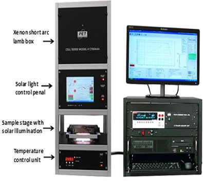
Class AAA solar simulator (for all the spectral match, non-uniformity of irradiation and temporal instability of irradiance) certified by all the standards, viz IEC, ASTM and JIS suitable for solar cell testing. The system have illumination housing, black finish to reduce the stray light, integrated shutter and power supply, irradiance monitoring, temperature sensors and safety interlocks. Setup can be used for the characterizations of Pphotodiodes, resistive switching memory and solar cells. Some of the specifications of the facilities as as follows:
- AM 1.5 G spectral matching.
- Area of illuminations 2 inch x 2inch
- Power output ≥ 100mW/cm2.
- Lamp power 400- 500 W with a line regulation 0.01%.
- Spectral range 400-1100 nm or more.
- I-V testing system with a current range of ~1uA to 1A with 0.5% accuracy, voltage range ~ 1nV to 20V with 0.05% accuracy.
- Computer/laptop with appropriate software to measure open circuit voltage VOC, short circuit current ISC, Vmax, Imax, Pmax, efficiency, fill factor, RSC, ROC and Rshunt.
- The software is capable to generate I-V curves as ASCII data and report I-V curve plot for fast data overview.
- NIST/NREL certified 2cm x2cm Si based photovoltaic reference cell for the calibration with meter to read 0 to 3.5 SUN, suitable temperature sensors and adapter cables for reference cell.
Publications
- “In Situ Study of Radiation Stability and Associated Conduction Mechanisms of Nb-Doped TiO2/p-Si Heterojunction Diode Under Swift Heavy Ion Irradiation.” Subodh Kumar Gautam, Jitendra Singh, Ram Gopal Singh, Naina Gautam, Priyanka Trivedi, Fouran Singh: IEEE Transactions on Electron Devices 66 (2019) 1475.
- “Multifunctional hybrid diode: Study of photoresponse, high responsivity, and charge injection mechanisms” J Singh, RG Singh, SK Gautam, Fouran Singh, Journal of Applied Physics 123 (17), 174503 2018.
- “Carrier transport mechanism of highly-sensitive niobium doped titanium dioxide/p-Si heterojunction photodiode under illuminations by solar simulated light,” S.K. Gautam, A. Das, R.G. Singh, V.V.S. Kumar, Fouran Singh, Journal of Applied Physics 120 (2016) 214502.
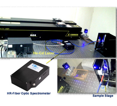
PL setup consists of He-Cd lasers (operating at two wavelengths: 325 nm @ 25 mW and 441.6 nm @ 88 mW) and a high resolution spectrometer from Ocean Optics (HR4000) coupled with charged coupled device (CCD) detector to record the spectrum in the range of 200 to 1100 nm. Figures shows the schematic diagram of PL set up at IUAC. PL is a sensitive and convenient technique for optical characterization of semiconductor materials such as semiconductors, organic materials, nanophosphors and defects in insulators and very useful to study the nature of the involved electronic transitions. The measurements are possible only on thin films and pellets at room temperature.
List of important publications
- Structure and photoluminescence studies on ZnS:Mn nanoparticles, (2004) Journal of Applied Physics, 95 (2), pp. 656-660. Karar, N., Singh, F., Mehta, B.R.
- Agarwal, D.C., Kumar, A., Khan, S.A., Kabiraj, D., Singh, F., Tripathi, A., Pivin, J.C., Chauhan, R.S., Avasthi, D.K. SHI induced modification of ZnO thin film: Optical and structural studies (2006) Nuclear Instruments and Methods in Physics Research, Section B: Beam Interactions with Materials and Atoms, 244 (1), pp. 136-140.
- Kumar, M., Singh, V.N., Singh, F., Lakshmi, K.V., Mehta, B.R., Singh, J.P. On the origin of photoluminescence in indium oxide octahedron structures (2008) Applied Physics Letters, 92 (17), art. no. 171907.
- Kumar, P.M.R., Kartha, C.S., Vijayakumar, K.P., Singh, F., Avasthi, D.K., Abe, T., Kashiwaba, Y., Okram, G.S., Kumar, M., Kumar, S. Modifications of ZnO thin films under dense electronic excitation (2005) Journal of Applied Physics, 97 (1), art. no. 013509.
- Singh, R.G., Singh, F., Agarwal, V., Mehra, R.M. Photoluminescence studies of ZnO/porous silicon nanocomposites (2007) Journal of Physics D: Applied Physics, 40 (10), art. no. 012, pp. 3090-3093.
- Kumar, M., Singh, F., Khan, S.A., Baranwal, V., Kumar, S., Agarwal, D.C., Siddiqui, A.M., Tripathi, A., Gupta, A., Avasthi, D.K., Pandey, A.C. Swift heavy ion induced structural and optical modifications in LiF thin film (2005) Journal of Physics D: Applied Physics, 38 (4), pp. 637-641.
- Pandey, A., Sahare, P.D., Bakare, J.S., Lochab, S.P., Singh, F., Kanjilal, D. Thermoluminescence and photoluminescence characteristics of nanocrystalline LiNaSO4:Eu phosphor (2003) Journal of Physics D: Applied Physics, 36 (19), pp. 2400-2406.
- Prashantha, S.C., Lakshminarasappa, B.N., Singh, F. 100 MeV Si 8 ion induced luminescence and thermoluminescence of nanocrystalline Mg 2SiO 4:Eu3 (2012) Journal of Luminescence, 132 (11), pp. 3093-3097.
- Pivin, J.C., Roger, G., Garcia, M.A., Singh, F., Avasthi, D.K. Nucleation and growth of Ag clusters in silicate glasses under ion irradiation (2004) Nuclear Instruments and Methods in Physics Research, Section B: Beam Interactions with Materials and Atoms, 215 (3-4), pp. 373-384.
- Singh, R.G., Singh, F., Kumar, V., Mehra, R.M. Growth kinetics of ZnO nanocrystallites: Structural, optical and photoluminescence properties tuned by thermal annealing (2011) Current Applied Physics, 11 (3), pp. 624-630.
- Siva Kumar, V.V., Singh, F., Kumar, A., Avasthi, D.K. Growth of ZnO nanocrystals in silica by rf co-sputter deposition and post-annealing (2006) Nuclear Instruments and Methods in Physics Research, Section B: Beam Interactions with Materials and Atoms, 244 (1), pp. 91-94.
- Tripathi, B., Singh, F., Avasthi, D.K., Das, D., Vijay, Y.K. Study of effects of Mn2+ in CdS nanocrystals, (2007) Physica B: Condensed Matter, 400 (1-2), pp. 70-76.
- Kumar, P., Saxena, N., Chandra, R., Gao, K., Zhou, S., Agarwal, A., Singh, F., Gupta, V., Kanjilal, D. SHI induced enhancement in green emission from nanocrystalline CdS thin films for photonic applications (2014) Journal of Luminescence, 147, pp. 184-189.
- Tripathi, B., Vijay, Y.K., Wate, S., Singh, F., Avasthi, D.K. Synthesis and luminescence properties of manganese-doped ZnS nanocrystals (2007) Solid-State Electronics, 51 (1), pp. 81-84.
- Mohanty, T., Mishra, N.C., Singh, F., Bhat, S.V., Kanjilal, D. Color center formation in sapphire by swift heavy ion irradiation, (2003) Radiation Measurements, 36 (1-6 SPEC.), pp. 723-727.
- Jheeta, K.S., Jain, D.C., Kumar, R., Singh, F., Garg, K.B. Photoluminescence study of swift heavy ion (SHI) induced defect centers in sapphire, (2006) Journal of Nuclear Materials, 353 (3), pp. 190-192.
- Lakshminarasappa, B.N., Shivaramu, N.J., Nagabhushana, K.R., Singh, F., Synthesis characterization and luminescence studies of 100 MeV Si 8+ ion irradiated sol gel derived nanocrystalline Y2O3, (2014) Nuclear Instruments and Methods in Physics Research, Section B: Beam Interactions with Materials and Atoms, 329, pp. 40-47.
- Nagabhushana, K.R., Lakshminarasappa, B.N., Singh, F., Photoluminescence and Raman studies in swift heavy ion irradiated polycrystalline aluminum oxide, (2009) Bulletin of Materials Science, 32 (5), pp. 515-519.
- Sunitha, D.V., Nagabhushana, H., Singh, F., Nagabhushana, B.M., Sharma, S.C., Chakradhar, R.P.S., Thermo, Iono and photoluminescence properties of 100 MeV Si 7 ions bombarded CaSiO3:Eu3+ nanophosphor, (2012) Journal of Luminescence, 132 (8), pp. 2065-2071
- Singh, R.G., Singh, F., Sulania, I., Kanjilal, D., Sehrawat, K., Agarwal, V., Mehra, R.M., Electronic excitations induced modifications of structural and optical properties of ZnO-porous silicon nanocomposites, (2009) Nuclear Instruments and Methods in Physics Research, Section B: Beam Interactions with Materials and Atoms, 267 (14), pp. 2399-2402.
- Kumar, P., Saxena, N., Gupta, V., Singh, F., Agarwal, A., Correlation between surface phonon mode and luminescence in nanocrystalline CdS thin films: An effect of ion beam irradiation, (2014) Journal of Applied Physics, 116 (4), art. no. 043517.
- Nagabhushana, H., Lakshminarasappa, B.N., Singh, F., Avasthi, D.K., Photoluminescence studies in swift heavy ion bombarded mullite, (2003) Nuclear Instruments and Methods in Physics Research, Section B: Beam Interactions with Materials and Atoms, 211 (4), pp. 545-548.
- Sehrawat, K., Singh, F., Singh, B.P., Mehra, R.M., Ion beam modification of porous silicon using high energy Au+7 ions and its impact on photoluminescence spectra, (2004) Journal of Luminescence, 106 (1), pp. 21-29.
- Lokesha, H.S., Nagabhushana, K.R., Singh, F., Luminescence properties of 100 MeV swift Si7+ ions irradiated nanocrystalline zirconium oxide, (2015) Journal of Alloys and Compounds, 647, art. no. 34562, pp. 921-926.
- Nagabhushana, K.R., Lakshminarasappa, B.N., Narasimha Rao, K., Singh, F., Sulania, I., AFM and photoluminescence studies of swift heavy ion induced nanostructured aluminum oxide thin films, (2008) Nuclear Instruments and Methods in Physics Research, Section B: Beam Interactions with Materials and Atoms, 266 (7), pp. 1049-1054.
- Nagabhushana, H., Prashantha, S.C., Lakshminarasappa, B.N., Singh, F., Ionoluminescence and photoluminescence studies of Ag8+ ion irradiated kyanite, (2008) Journal of Luminescence, 128 (1), pp. 7-10.
- Nagabhushana, K.R., Lakshminarasappa, B.N., Chandrappa, G.T., Haranath, D., Singh, F., Swift heavy ion induced photoluminescence studies in Aluminum oxide, (2007) Radiation Effects and Defects in Solids, 162 (5), pp. 325-332.
- Shivaramu, N.J., Nagabhushana, K.R., Lakshminarasappa, B.N., Singh, F., Ion beam induced luminescence studies of sol gel derived Y2O3:Dy3+ nanophosphors, (2016) Journal of Luminescence, 169, pp. 627-634.
- Bedyal, A.K., Kumar, V., Sharma, V., Singh, F., Lochab, S.P., Ntwaeaborwa, O.M., Swart, H.C., Swift heavy ion induced structural, optical and luminescence modification in NaSrBO3:Dy3+ phosphor, (2014) Journal of Materials Science, 49 (18), pp. 6404-6412.
- Kumar, Y., Herrera-Zaldivar, M., Olive-Méndez, S.F., Singh, F., Mathew, X., Agarwal, V., Modification of optical and electrical properties of zinc oxide-coated porous silicon nanostructures induced by swift heavy ion, (2012) Nanoscale Research Letters, 7, pp. 2-17.
- Singh, R.G., Singh, F., Mehra, R.M., Kanjilal, D., Agarwal, V., Synthesis of nanocrystalline α - us silicon interface: Phase transition study, (2011) Solid State Communications, 151 (9), pp. 701-703.
- Shivaramu, N.J., Lakshminarasappa, B.N., Nagabhushana, K.R., Singh, F., Luminescence studies of 100 MeV Si8+ ion irradiated nanocrystalline Y2O3, (2014) Radiation Measurements, 71, pp. 518-523.
- Premkumar, H.B., Sunitha, D.V., Singh, F., Nagabhushana, H., Sharma, S.C., Nagabhushana, B.M., Zhao, G., Chen, J., Chakradhar, R.P.S., Luminescence and defect studies of YAlO 3:Dy 3+, Sm 3+ single crystals exposed to 100 MeV Si 7+ ion beam, (2012) Journal of Luminescence, 132 (10), pp. 2679-2683.
- Nagabhushana, H., Umesh, B., Nagabhushana, B.M., Lakshminarasappa, B.N., Singh, F., Chakradhar, R.P.S., Determination of the chemical states of impurities in natural kyanite by the ionoluminescence technique, (2009) Philosophical Magazine, 89 (11), pp. 995-1004.
- Kumar, M., Singh, F., Khan, S.A., Tripathi, A., Avasthi, D.K., Pandey, A.C., Studies of swift heavy ion induced colour centres in LIF thin films deposited on silica substrates, (2006) Journal of Physics D: Applied Physics, 39 (14), art. no. 010, pp. 2935-2940.
- Nagabhushana, K.R., Lakshminarasappa, B.N., Revannasiddaiah, D., Singh, F., Luminescence studies on swift heavy ion irradiated nanocrystalline aluminum oxide, (2011) Journal of Luminescence, 131 (4), pp. 764-767.
- Sunitha, D.V., Nagabhushana, H., Singh, F., Dhananjaya, N., Sharma, S.C., Nagabhushana, B.M., Shivakumara, C., Chakradhar, R.P.S., Swift heavy ion induced structural, iono and photoluminescence properties of β-CaSiO 3:Dy 3+ nanophosphor, (2012) Spectrochimica Acta - Part A: Molecular and Biomolecular Spectroscopy, 93, pp. 300-305.
- Kumar, A., Singh, F., Pivin, J.C., Avasthi, D.K., Photoluminescence studies of carbon clusters formed by irradiation of Si-based polymer, (2005) Radiation Measurements, 40 (2-6), pp. 785-788.
- Baranwal, V., Krishna, R., Singh, F., Tripathi, A., Pandey, A.C., Kanjilal, D., Synthesis of GaN phase by ion implantation, (2007) Applied Surface Science, 253 (12), pp. 5317-5319.
- Mohanta, D., Ahmed, G.A., Choudhury, A., Singh, F., Avasthi, D.K., Properties of 80-MeV oxygen ion irradiated ZnS:Mn nanoparticles and exploitation in nanophotonics, (2006) Journal of Nanoparticle Research, 8 (5), pp. 645-652.
- Singh, F., Sarma, A., Montereali, R.M., Bonfigli, F., Baldacchini, G., Avasthi, D.K., Optical absorption and photoluminescence studies on thin films and bulk crystals of LiF under swift heavy ion irradiation, (2003) Radiation Measurements, 36 (1-6 SPEC.), pp. 675-679.
- Nagabhushana, H., Umesh, B., Nagabhushana, B.M., Lakshminarasappa, B.N., Singh, F., Chakradhar, R.P.S., Photoluminescence studies of 100 MeV Ni8+ ion irradiated Al2O3 single crystals, (2009) Spectrochimica Acta - Part A: Molecular and Biomolecular Spectroscopy, 73 (4), pp. 637-641.
- Lokesha, H.S., Nagabhushana, K.R., Singh, F., Enhancement in luminescence properties of ZrO2:Dy3+ under 100 MeV swift Ni7+ ion irradiation, (2016) RSC Advances, 6 (60), pp. 55240-55247.
- Kumar, Y., Herrera, M., Singh, F., Olive-Méndez, S.F., Kanjilal, D., Kumar, S., Agarwal, V., Cathodoluminescence and photoluminescence of swift ion irradiation modified zinc oxide-porous silicon nanocomposite, (2012) Materials Science and Engineering B: Solid-State Materials for Advanced Technology, 177 (16), pp. 1476-1481.
- Nagabhushana, H., Prashantha, S.C., Nagabhushana, B.M., Lakshminarasappa, B.N., Singh, F., Chakradhar, R.P.S., Ion beam-induced luminescence and photoluminescence of 100 MeV Si8+ ion irradiated kyanite single crystals, (2008) Solid State Communications, 147 (9-10), pp. 377-380.
- Nagabhushana, H., Lakshminarasappa, B.N., Singh, F., Avasthi, D.K., Ionoluminescence and photoluminescence in swift heavy ion-irradiated Al2SiO5, (2003) Radiation Measurements, 36 (1-6 SPEC.), pp. 643-646.
- Jheeta, K.S., Jain, D.C., Singh, F., Kumar, R., Garg, K.B., Photoluminescence and UV-vis studies of pre- and post-irradiated sapphire with 200 MeV Ag8+ ions, (2006) Nuclear Instruments and Methods in Physics Research, Section B: Beam Interactions with Materials and Atoms, 244 (1), pp. 187-189.
- Tripathi, B., Vijay, Y.K., Singh, F., Avasthi, D.K., Wate, S., Study of C6+ (80 MeV) ion induced effects on CdS:Mn system, (2008) Journal of Alloys and Compounds, 459 (1-2), pp. 118-122.
- Shivaramu, N.J., Lakshminarasappa, B.N., Singh, F., Coetsee, E., Swart, H.C., Photoluminescence, thermoluminescence and defect centres in Y2O3 and Y2O3:Tb3+ under 100 MeV swift Ni8+ ion beam irradiation, (2018) Materials Research Bulletin, 102, pp. 62-69.
- Premkumar, H.B., Sunitha, D.V., Nagabhushana, H., Sharma, S.C., Prashantha, S.C., Singh, F., Nagabhushana, B.M., Zhao, G., Chen, J., Chakradhar, R.P.S., Heavy ion induced luminescence studies of YAlO3: Tb3+, Tm3+ single crystals, (2014) Materials Research Express, 1 (1), art. no. 015908.
- Agarwal, D.C., Kabiraj, D., Singh, F., Avasthi, D.K., Pellegrini, G., Chandra, R., Mazzoldi, P., Synthesis of ZnO nanostructures using different metal catalyst: Morphology and photoluminescence characteristics, (2010) Journal of Nanoscience and Nanotechnology, 10 (4), pp. 2933-2937.
- Kumar, M., Rajput, P., Singh, P.K., Yadav, A.C., Pradhan, S.L., Baranwal, V., Singh, U.B., Jha, S.N., Singh, F., Luminescence properties of BaMgAl10O17: Mn2+ nanophosphors, (2019) Journal of Alloys and Compounds, 799, pp. 556-562.
- Bharti, M.L., Singh, F., Ramola, R.C., Joshi, V., Photoluminescence and reflectivity studies of high energy light ions irradiated polymethyl methacrylate films, (2017) Optical Materials, 73, pp. 550-554.
- Kumar, P., Saxena, N., Singh, F., Gupta, V., Swift heavy ion induced structural phase generation and enhanced luminescence from CdS based nanocomposites, (2016) Surface and Coatings Technology, 306, pp. 305-308.
- Nagabhushana, H., Singh, F., Sharma, S.C., Nagabhushana, B.M., Chakradhar, R.P.S., Ionoluminescence studies of natural kyanite mineral from different parts of Indian origin, (2012) Spectrochimica Acta - Part A: Molecular and Biomolecular Spectroscopy, 86, pp. 15-19.
- Das, U., Mohanta, D., Singh, F., Tripathi, A., Avasthi, D.K., Choudhury, A., Transition metal doped ZnS nanoparticle systems and their response to swift heavy ion irradiation, (2007) Indian Journal of Physics, 81 (1), pp. 155-159.
- Bhardwaj, D.M., Jain, D.C., Rao, K.V.R., Kumar, R., Singh, F., Gupta, R.P., Photoluminescence and atomic force microscopic studies on pre- and post-irradiated ruby with Ni6+ ion, (2004) Nuclear Instruments and Methods in Physics Research, Section B: Beam Interactions with Materials and Atoms, 222 (3-4), pp. 533-537.
- Kumar, S., Shah, S., Sulania, I., Singh, F., Chakraborty, A., Structural investigation of low energy ion irradiated Al2O3, (2019) Ceramics International, 45 (16), pp. 20346-20353.
- Satyanarayana Reddy, S., Nagabhushana, K.R., Singh, F., Structure and crystal field analysis using ionoluminescence of Al2O3: Tm3+ phosphor, (2019) Journal of Luminescence, 214, art. no. 116553.
- Kumar, M., Rajput, P., Singh, P.K., Yadav, A.C., Khan, S.A., Jha, S.N., Singh, F., Pandey, A.C., Europium activated gadolinium sulfide nanoparticles, (2016) RSC Advances, 6 (110), pp. 108523-108529.
- Bhardwaj, D.M., Jain, D.C., Garg, K.B., Kumar, R., Singh, F., Gupta, R.P., Photoluminescence and atomic force microscopy studies on pre- and post-irradiated ruby with Fe3+ ion, (2004) Radiation Effects and Defects in Solids, 159 (5), pp. 315-320.
Ultraviolet-Visible-Near infrared (UV-Vis-NIR) facility is equipped with Hitachi-4150 spectrophotometer and capable of measurements in the range of 200-2400 nm. Measurements are being carried out with integrating sphere. Spectrometer is capable of doing measurements in the reflection mode as well. The data is acquired with the software UV- solution and samples are mounted onto the sample holder such a manner that the sample should cover the hole of the holder and Place sample holder into the sample compartment. Before starting any measurement do the baseline correction by single click on baseline command given at the right side of the screen and then select that baseline for those series of measurements. After baseline correction, set the analytical parameters as for your sample requirements and measurements are started.
Fourier Transform infrared (FTIR) from Bruker (VORTEX70) can be used to the measurements in the range of 100-6000 cm-1. The thin films, powders and polymers can be measured. The data is acquired with the OPUS software and we need to make sure there is no error message and dry gas flow is normal before starting the measurements. The samples are mounted onto the sample holder and placed it into the sample compartment. The analytical parameters are set as per your sample requirement of the measurements.
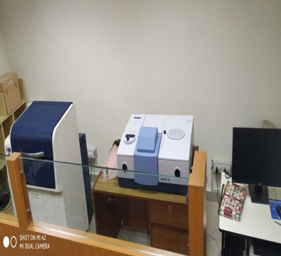
Photo-induced inter-chain and interfacial charge transfer in Cu–ZnO/poly (3-octylthiophene) hybrid nanocomposites, J Singh, RG Singh, H Gupta, S Ojha, F Singh, Optical Materials 94 (2019) 316.
A SPEX CertiPrep 8000D Dual Mixer/Mill has been installed and used for synthesis of nanopowder materials. Hardened steel, Agate and Silicon Nitride vials are available for pulverizing Ferrite and semiconductor materials. This system can also be used for mechanical alloying of powder materials. Nanopowders of Mn0.4Zn0.6Fe2O4, Bi doped BaS, Ce doped SrS, Y23Fe5O12, SiO2 were prepared by pulverizing their powder materials and nanopowders of Boron-Carbon-Nitride (BN + Graphite ) and SiC (Si + Graphite ) were prepared by mechanical alloying.
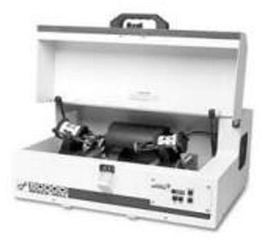
An indigenously developed rf sputtering system is being used regularly for the deposition of thin films. The system includes:
- RF power supply: Indigenously developed 500 W, 13.56 MHz with matching network.
- Stainless steel deposition chamber with water cooled target holders for 2 inch and 4 inch diameter targets, grounded anode, view port, and ports for vacuum components, gas flow, shutter and electrical feedthroughs.
- Vacuum system: Turbo pump/Dry pump used to produce clean vacuum, Penning and pirani gauges used for measuring the vacuum.
- Gas flow: MKS MFC’s used to feed gas into the chamber at set flow rates.
- Manual gate valve used as throttle valve to set the deposition pressure in combination with the gas flow rates.
- Substrate heater: 2 inch diameter substrate holder with K type Thermocouple, radiation shield and heating upto 600°C.
Argon, Oxygen and nitrogen gases can be used to grow thin films of metals, oxides and nitrides. Thin films of ZnO, ZnO/SiOx nanocomposites, ZnS, ZnS/SiOx nanocomposite, Ni, Mg-Mn Ferrites, Strontium Barium Niobate, CeO2 , Hydroxyapatite, Copper nitride, Boron-Carbon-Nitride etc. have been synthesized for performing ion beam irradiation studies.
Another RF Sputtering system available with the group has the following features:
- Three cathodes.
- RF Power 100 W.
- Arrangement for substrate heating.
- Quartz crystal thickness monitor.
- Pumped by a turbo molecular pump.
- * Base pressure ~10-7 mbar.
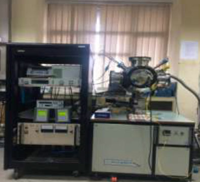
- “In Situ Study of Radiation Stability and Associated Conduction Mechanisms of Nb-Doped TiO2/p-Si Heterojunction Diode Under Swift Heavy Ion Irradiation.” Subodh Kumar Gautam, Jitendra Singh, Ram Gopal Singh, Naina Gautam, Priyanka Trivedi, Fouran Singh: IEEE Transactions on Electron Devices 66 (2019) 1475.
- “Carrier transport mechanism of highly-sensitive niobium doped titanium dioxide/p-Si heterojunction photodiode under illuminations by solar simulated light,” S.K. Gautam, A. Das, R.G. Singh, V.V.S. Kumar, Fouran Singh, Journal of Applied Physics 120 (2016) 214502.
One of the thermal evaporation systems available with the group has the following features:
- Four pocket electron beam gun.
- Arrangement for resistive heating.
- Quartz crystal thickness monitor.
- Pumped by a turbo molecular pump.
- Base pressure ~10-7 mbar.
